Abstract
Novel architectures of transparent electrodes incorporating graphene into its design are explored to improve the silicon-heterojunction-cell technology. Two configurations are studied based on the place where the atomic graphene is. The main results obtained reveal the dramatic dependence of atomic graphene position on the transparent-electrode properties. In addition, the electrode performance is also affected by the transparent conductive oxide material chosen in the designed structure. Specifically, the incorporation of graphene into an electrode shows a significant reduction of its sheet resistance (55 Ω/sq.) and the weighted reflectance of whole structure down up to 10% when combined with a transparent conductive oxide such as indium tin oxide. Such electrode shows an average conductance value as high as 13.12 mS. These data undergone so far clearly suggest the possibility to noticeably improve transparent electrode technology when graphene is incorporated, and therefore to further enhance the contact technology for solar cells.
Keywords
graphene, transparent conductive oxides, front-electrode, solar devices.
Introduction
The exceptional properties of graphene, a two dimensional version of carbon, turn this material into very attractive from both companies and research groups since the publication of pioneering work by Novoselov et al. [1]. Its high thermal conductivity, its excellent mechanical properties, its huge specific surface area and its exceptional electronic conductivity make graphene a promising candidate for a large field of applications such as displays, touch screens or solar cells [2-4].
On the other hand, photovoltaic (PV) technology is expected to play a major role in the renewable-energy sector because of the fight against the climate change. This climate action has as its main aim to reduce greenhouse gas emissions. The targets defined by European Union within the framework of “Clean Energy for All European package” reflect the need for changing markets dynamics in the energy sector, considering the PV sector as one of the most involved in this issue [5]. PV market is currently being dominated by silicon-wafer technology in a 90%. This sector requires exhaustive technological solutions to achieve thinner and cheaper products. In this sense, silicon-heterojunction (SHJ) technology is emerging as a low-temperature reliable solution, where new architectures of transparent conductive electrodes to generate and extract the current in a more efficient way are required [6]. In this sense, this work presents the development of a novel transparent electrode that incorporates graphene with the main aims of exploring its possible advantages and improving solar cell performance.
Methods and materials
The transparent conductive electrodes (TCEs) are based on the combination between atomic graphene and a transparent conductive oxide (TCO). In this design, the graphene would help to improve the electrical properties, and the TCO would play the role of antireflective layer (AR), essential property for the specific application in SHJ technology.
The synthesis of graphene was carried out by chemical vapour deposition (CVD) using a commercial cold-wall CVD reactor from Aixtron. All the process gases (argon (Ar), hydrogen (H2), and methane (CH4)) were flushed before the growth. The temperature was then raised to 1050°C under Ar atmosphere. Once the temperature was stabilized, a mixture of 0.7 % CH4 / 31% H2 / 68.3 % Ar (in volume) was introduced for 15 minutes at 50 mbar of pressure. The synthesized graphene on the Cu foil was transferred to the different substrates using a home-built system designed to automatically transfer graphene [7].
The TCO materials were fabricated at low temperature using a commercial UNIVEX 450B sputtering system with confocal geometry from Leybold. The gas used in the sputtering process was Ar with a purity of 99.999%, and its flux was controlled with a mass-flow controller. The choice of TCO materials was aluminum-doped zinc oxide (AZO), from 4-inch ZnO:Al2O3 (98/2 wt.%, Neyco) commercial ceramic target operated by Radio-Frequency (RF), and indium tin oxide (ITO) from 4-inch In2O3: SnO2 (90/10 wt.%, Neyco) commercial ceramic target operated by Direct Current (DC).
The TCE performance is determined by analysing the electrical and optical properties. From electrical point of view, the sheet resistance and conductivity are evaluated from a mapping of electrical conductance carried out using a non-contact and non-destructive commercial Onyx system from Das Nano Company, based on reflection-mode terahertz time-domain spectroscopy (THz-TDS). Finally, the optical analysis consists on the evaluation of the AR capability of the TCE. This AR capability was determined from the analysis of weighted reflectance Rp defined as,
where Rhem is the hemispherical reflectance measured by using a UV/Visible/NIR Perkin-Elmer Lambda 1050 spectrophotometer equipped with a 6 mm integrating sphere accessory; and e(λ) is the global spectral AM1.5G irradiance.
Results and discussion
The challenges of introducing graphene in the TCE structure were evaluated. Two different configurations were studied: configuration 1, where the atomic graphene was transferred on top of sputtered TCO-on-substrate (crystalline silicon); and configuration 2, where the TCO was sputtered on top of the atomic graphene, transferred directly onto the crystalline silicon. It was found that the compatibility between the process temperatures required in each step was extremely relevant into the electrode performance. For this reason, the transfer process was carried out at room temperature; thereby, a possible damage into the TCO layer would be avoided. In addition, the dependence of the place where the atomic graphene was located and the number of monolayers transferred were also crucial. The effect of sputtering deposition parameters on the electrical electrode performance was checked carefully. As the first choice, the TCO used in the design was an 80nm-thick AZO thin film. Measured electrical data of the TCEs fabricated incorporating up to three graphene monolayers at different places are pictured in Figure 1. It can be observed that the measured sheet resistances were far from the theoretical ones (straight line). More precisely, the sheet resistances of TCE fabricated with configuration 1 were far lower than those measured in the TCEs with configuration 2. This was attributed to the huge damage produced in the graphene atomic order because of the bombardment generated during sputtering process [8]. This fact would be making possible to exclude the configuration 2 from the study. With regard to the number of graphene monolayers, any preliminary conclusion may be determined from the experimental results. On contrary, from the theoretical point of view, an improvement of the sheet resistance would be expected with each graphene monolayer incorporated. As summary from these preliminary experimental electrical results, the optimum TCE design would be that one in which the atomic graphene was placed on top of TCO material, named configuration 1 in this work.
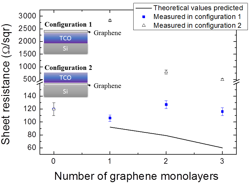
Figure 1. TCE’s sheet resistance measured as function of number of monolayers incorporated in the design, depending on its place (configuration 1: monolayer graphene transferred on top of TCO; configuration 2: TCO sputtered on top of graphene). In this case, the TCO incorporated into the design was an 80 nm-thick AZO layer. As comparison, theoretical values are also included.
The next step was to determine which TCO material was more appropriated to be used in the TCE structure. Taking theoretical sheet resistances into account (showed as a straight line in
Figure 1), three graphene monolayers were used. Table 1 shows the sheet resistance values of TCEs fabricated as function of the TCO material used. As these data revealed, a strong effect was observed depending on the TCO incorporated in the structure, reaching ~55 Ω/sq. with ITO versus ~116 Ω/sq. with AZO. This difference was attributed to the possible aluminum diffusion from the AZO layer into graphene monolayers. This aluminum diffusion would lead to the formation of other compounds, such as aluminum carbide, affecting the graphene order and hence, the electrical parameters [9]. As conclusion, the electrical performance was considerably improved using an aluminum-free TCO material, just as in the case of ITO.
Table 1. Measured sheet resistances of the TCEs fabricated in configuration 1.
|
TCO Material |
Graphene monolayers |
Rsheet (Ω/sq.) |
|
ITO |
3 |
55 ± 5 |
|
AZO |
3 |
116 ± 6 |
Figure 2 shows the THz-TDS conductance and resistance maps acquired in reflection-mode for the TCE based on three graphene monolayers transferred on top of 80 nm-thick ITO thin film. It can be appreciated a central region with an average conductance of 13.12 mS, and a maximum value of 14.03 mS measured in the center of the sample. A region of lower conductivity close to 10-12 mS was observed in the edge of sample, attributed to the edge effect of graphene transfer. The average conductance value of 13.12 mS was considerably higher than the measured one of a common TCO, ~10mS, making the TCE presented here an alternative and competitive front-electrode [10]. In addition, from the resistance map, a sheet resistance of 76.2 Ω/sq. was extracted in the center region of the sample, slightly higher than the measured one using conventional transmission line method.
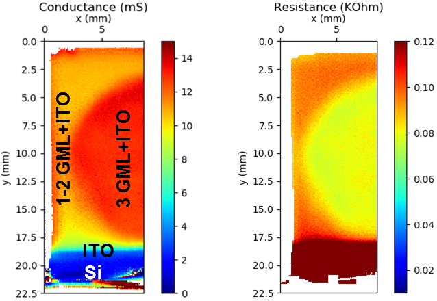
Figure 2. THz-TDS conductance and resistance maps acquired in reflection-mode for the optimum TCE based on three graphene monolayers transferred on top of 80nm-thick ITO thin film sputtered on crystalline silicon.
With regard to optical properties, Figure 3 pictures the total (hemispherical) reflectance measured with the integrated sphere of two TCEs based on AZO and ITO, respectively. It should be noted that the combination of graphene with a TCO reduced the weighted reflectance of the whole TCE, close to 10%, providing a better AR capability than a bare common TCO (~12%). This superior AR capability is considered as very promising result that could be advantageous for SHJ technology, reducing the amount of light reflected and hence, improving the solar cell performance.
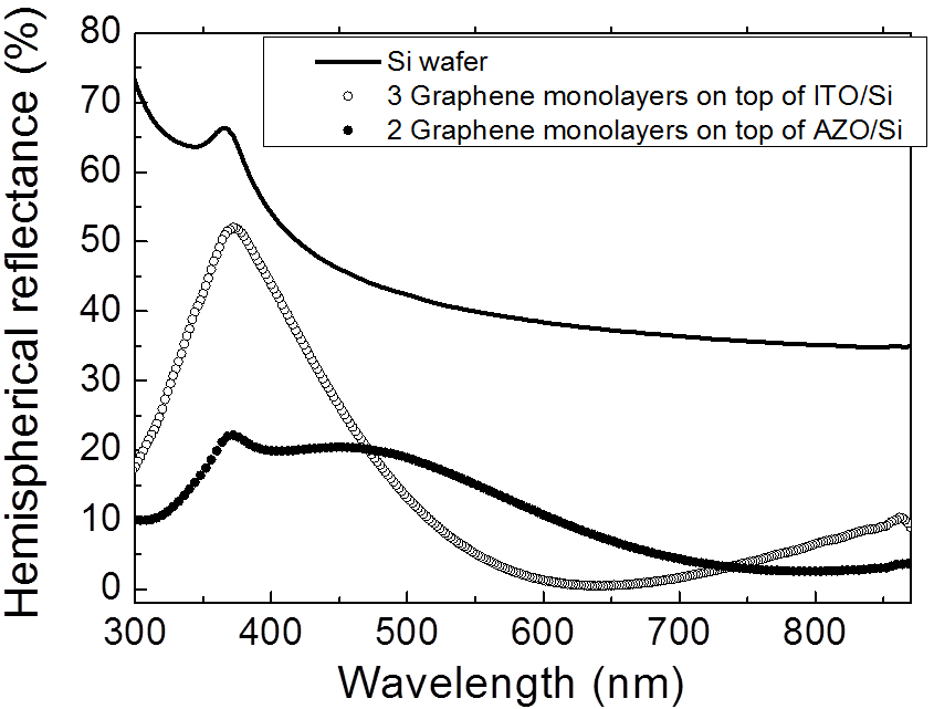
Figure 3. Total (hemispherical) reflectance spectra in the visible range (300-875 nm) of a system of two graphene monolayers stacked on top of a 80 nm-thick AZO film on crystalline silicon (fill circle symbol), on top of 80 nm-thick ITO film on crystalline silicon (open circle symbol), and the bare crystalline silicon wafer (straight line).
Finally, taking the electrical and optical properties studied into account, the optimized TCE is based on three graphene monolayers transferred on top of 80 nm-thick ITO. This result clearly suggests the possibility to improve the TCEs with the incorporation of graphene, and therefore, to further enhance the SHJ technology performance.
Conclusions
In this work, the key parameters for choosing the most appropriated and reliable combination of TCE were determined. Firstly, the compatibility of the TCO and graphene fabrication processes was analysed. The choice of the most appropriate TCO material was studied, observing a negative influence on electrical properties when TCO was based on aluminum. Hence, it was demonstrated the excellent performance of a TCE based on three graphene monolayers transferred on top of 80 nm-thick ITO thin films sputtered on crystalline silicon. This is a very attractive result that allows predicting that the incorporation of graphene to a cell’s front electrode could be very benefit on (i) the reduction of silicon-heterojunction transparent-electrode sheet resistances, and (ii) the decrease of the cell’s reflectance, favouring the absorption of more photons.
Acknowledgements
Authors acknowledge the partial financial support provided by the Spanish Ministry of Science & Innovation under the project DIGRAFEN (ENE2017-88065-C2-1-R) and (ENE2017-88065-C2-2-R); A. Inés and I. Arnedo acknowledges the financial support provided by FEDER and the Spanish Ministry of Science, Innovation and Universities – State Research Agency, under the project TEC2017-85529-C3-2-R (AEI/FEDER, UE).
References
- Novoselov KS, Geim AK, Morozov SV, Jiang D, et al. (2004) Electric Field Effect in Atomically Thin Carbon Films. Science.
- Pang S, Hernandez Y, Feng X, Müllen K (2011) Graphene as transparent electrode material for organic electronics. Adv. Mater.
- Ahn JH, Hong BH (2014) Graphene for displays that bend. Nature Nanotech.
- Zang Y, Li LB, Chu Q, Pu H, et al. (2018) Graphene as transparent electrode in Si solar cells: A dry transfer method. AIP Advances.
- Web page. Available: https://ec.europa.eu/energy/en/topics/energy-strategy-and-energy-union/clean-energy-all-europeans
- Green MA, Emery K, Hishikawa Y, Warta, et al. (2017) Solar cell efficiency tables (version 49). Prog. Photovolt: Res. Appl.
- Bosca A, Pedrós J, Martínez J, Palacios T, et al. (2016) Automatic Graphene transfer system for improved material quality and efficiency. Scientific Reports.
- Qiu XP, Shin YJ, Niu J, Kulothungasagaran N, et al. (2012) Disorder-free sputtering method on graphene. AIP Advances
- Rashad, M, Pan, F, Yu, Z, Asif, M, et al. (2015) Investigation on microstructural, mechanical and electrochemical properties of aluminum composites reinforced with graphene nanoplatelets. Prog. Nat. Sci.-Mater.
- Bøggild P, Mackenzie DMA, Whelan PR, Petersen DH, et al. (2017) Mapping the electrical properties of large-area graphene. 2D Materials.