Abstract
To date, solar energy storage coupled with nanomaterials, surface engineering becomes an essentially critical method for functional electrode design. Despite years of research on nanoscale materials for energy storage, commercial batteries still make use of microscale materials for electrodes. This is due to a combination of manufacturing challenges for nanoscale materials and the reactive nature of nanoscale materials that leads to high irreversible capacities associated with solid electrolyte interphase formation.
Surface texturing is a powerful tool to decouple bulk material properties from surface characteristics that often bottleneck energy storage applications of nanomaterials and has been successfully used to improve the efficiency of photodetectors and solar cells due to a reduction in reflections at the surface.
Therefore, the simple surface texturing methods for green energy-silicon solar energy are marked aim to provide the vital information about the growing field related to surface engineering in solar energy with environmental friendly nature.
Keywords
Solar energy, Surface texturing, Green energy
Introduction
Solar energy, as a popular green energy, is radiant light and heat from the Sun. The large magnitude of solar energy available makes it a highly appealing source of electricity. The International Energy Agency has said that solar energy can make considerable contributions to solving some of the most urgent problems the world now faces: The development of affordable, inexhaustible and clean solar energy technologies will have huge longer-term benefits. It will increase countries’ energy security through reliance on an indigenous, inexhaustible and mostly import-independent resource, enhance sustainability, reduce pollution, lower the costs of mitigating climate change, and keep fossil fuel prices lower than otherwise. These advantages are global. Hence the additional costs of the incentives for early deployment should be considered learning investments; they must be wisely spent and need to be widely shared [1-5].
In a textured surface, rather than being lost, the reflected light can strike the silicon surface again to minimize reflection. Any “roughening” of the surface reduces reflection by increasing the chances of reflected light bouncing back onto the surface, rather than out to the surrounding air.
Photovoltaic Effect
The mechanism of solar energy is on the basis of photovoltaic effect. In simple terms, the photovoltaic effect describes the conversion of light into an electric current. To describe this mechanism more formally, it is best to think of light in terms of a stream of photons where each photon carries one quantum of energy. Each photon is associated with just one wavelength or frequency. High-frequency photons have more energy than the ones with low frequency [6-8].
Intrinsic Semiconductor
In a pure semi-conductor the outermost electron of the underlying molecule is not heavily bound. An incoming photon with enough energy can promote the electron from the valence band to become a free electron in the conduction band as shown in Figure 1. This in turn leaves a positive hole in the valence band. The minimum energy that is necessary for this to happen is called the band gap. The band gap varies from material to material and also varies with temperature, which is why performance of solar modules deteriorates with higher temperatures. However, in an intrinsic semiconductor, no resulting electric current is observed, since the promoted electrons re-combine again with the holes.
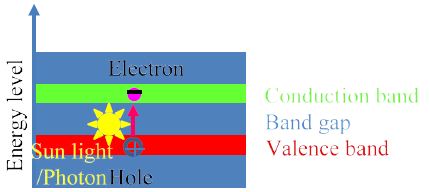
Figure 1: Schematic diagram of intrinsic semiconductor.
Doped Semiconductors
Doping means the addition of a small percentage of foreign atoms in regular crystal lattice of the semiconductor as shown in Figure 2.
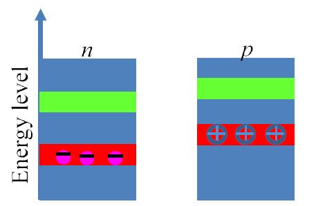
Figure 2: Schematic diagram of doped semiconductors.
n-Type
Adding atoms with one electron more creates a layer with more electrons in the valence band, pushing the overall energy level down. In Silicon, n-type dopants are Antimony, Arsenic or Phosphorous.
p-Type
Adding atoms with one electron less creates a layer with fewer negative electrons in the valence band, pushing the overall energy level up. For instance: In Silicon, add Boron, Aluminum or Gallium.
Semiconductor with p-n Junction
Where p-type and n-type layers join at the p–n junction, electrons and holes diffuse to create the charge-free depletion zone. Moreover, the junction creates a slope in the resulting energy bands. Now, when a photon promotes an electron to the conduction band, it can subsequently “roll down” through the depletion zone into a lower energy band rather than instantly re-combine with a hole. This is what generates the photo current as shown in Figure 3.
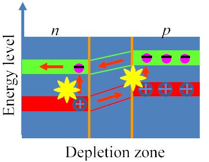
Figure 3: Schematic diagram of semiconductor with p–n junction.
Solar Cell Working Steps
It is well known that up to now, the most commonly known solar cell is configured as a large-area p–n junction made from silicon. Its working steps are listed as follows:
(i) Photons in sunlight hit the solar panel and are absorbed by semiconducting materials, such as silicon.
(ii) Electrons are excited from their current molecular/atomic orbital. Once excited an electron can either dissipate the energy as heat and return to its orbital or travel through the cell until it reaches an electrode. Current flows through the material to cancel the potential and this electricity is captured. The chemical bonds of the material are vital for this process to work, and usually silicon is used in two layers, these layers have different chemical electric charges and subsequently both drive and direct the current of electrons.
(iii) An array of solar cells converts solar energy into a usable amount of direct current (DC) electricity.
(iV) An inverter can convert the power to alternating current (AC).
Principle of Texturing for Antireflection
Energy conversion efficiency is a critical consideration in the application of solar cells, especially for the silicon solar cells. Texturing has been used as a technique to improve the efficiency of photodetectors and solar cells due to a reduction in reflections at the front surface.
The anti-reflecting features may be cones, pyramids, pillars, and other features, and, when such features are used for diffusion and for the scattering of light may they be distributed in a random fashion. It should be noted that any feature that produces the desired diffusive light scattering is one that closely approximates a Lambertian scattering surface at the desired wavelengths of radiation. Lambertian scattering is ideal diffuse scattering providing light distributed over the whole half sphere or solid angle of 2π steradians [9,10]. Manipulating the feature sizes, dimensions, etc. allows the light anti-reflecting and light diffusing region to be tunable for a specific wavelength. Varying the material near or deposited upon the anti-reflecting and light diffusing region can also be used to enhance these characteristics.
Texturing will also change the absorption in the remaining part of the infrared and the visible light regions but this will not yet be considered. In the near infrared the index of refraction of silicon is η = 3.42 and the reflectance is about R = 30% from a single surface and transmittance through a single surface is T = 70% for normal incident waves. The absorption coefficient of silicon is very low in the near infrared. If there is no backside reflector radiation under normal incidence is reflected first from the first surface. There are successive reflections from both the back and internal reflections from the front surface resulting in a total transmittance, if there is no reflective layer or the oxide layer, of
Ttot=(TT)(1+R2+R4+…)=(TT)/(1-R2)
This result has been obtained using the sum of a geometric series. If both top and back surfaces are just polished silicon–air then this results in a total transmittance of 54% and a reflectance of 46%. The internal absorption, A, of infrared light where the absorption coefficient, α, is very low due multiple internal reflections in a sample of thickness, d, with a polished backside is:
A=αd(1+R2)(1+R1R2+R12R22+…)=αd(1+R2)/(1-R1R2)
The enhancement, Enh, in internal absorption by multiple internal reflections with a polished backside is
Enh=(1+R2)/(1-R1R2)
One of the difficulties in silicon technology is realizing a backside reflector. Metal directly on a silicon backside has been found in practice not to be a good reflector. One approach in thin film technology has been to deposit silicon on an oxide over a textured metal. In doing so the desire has been to use thicker oxides to try to planarize the oxide top surface for silicon deposition. While the metal may be a diffusive reflector but the reflected light is refracted towards the normal upon entering the silicon. The light in the silicon will not appear to originate from a Lambertian scattering source. If the backside of the silicon is textured and a thin oxide or dielectric used before metal deposition, when the oxide is thin, much less than a quarter wave length then the reflected light is not affected by the thin oxide and the reflection into the silicon can be Lambertian scattering.
A random array of such etched “cusps” into the backside of a silicon wafer can be provided by porous silicon and chemical etches. A porous silicon or metal catalyst etch can provide vertical holes at random locations, these can then be etched with a conventional isotropic silicon etch to round off the shape corners resulting in a cusp like structure. A thin layer of oxide can either be grown or oxide or another dielectric deposited and the backside covered by a reflective metal. In this manner a random array of cusp like scattering centers can be formed on the back of silicon solar cells.
Starting with the 1990s, silicon solar cells with 23.4% efficiency have been obtained. One of the known ways to increase the conversion efficiency is the reducing of the radiation losses at the front surface of the cell. There have been reported various methods of increasing silicon solar cell efficiency by improving the structure light trapping such as: rear surface preparation to assure the reflection of unabsorbed light at the first path through structure and front surface texturing reducing the surface reflection to the maximum [11-14]. Front surface texturing of single crystalline silicon cells depends on the etching solution that can be isotropic or anisotropic, on the crystallography orientation, <100> or <111> of the silicon wafers and on the etching mask geometry [15].
Common Processes of Fabrication of Texturing Surfaces to Obtain an as-low-as-Possible Reflectance
Optical Lithography
Silicon wafer surface texturing has been realized using MEMS technology [16]. The technological flow is shown in Figure 4.
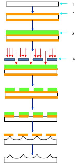
Figure 4: Technological flow for texturing surface realization: (1) silicon wafer, (2) silicon dioxide layer used as a masking layer for etching, (3) positive photoresist and (4) photolithographic process using mask.
The first step of the technological flow presented is the growth of a silicon dioxide layer used as a masking layer for etching. In the next step, by a photolithographic process based on positive photoresist, the patterned holes in silicon dioxide are formed.
Figure 5 shows the image of the surface etched in the (HNO3:HF-50:1) solution, where Figure 5(a) presents a perspective view of the texturized surface while Figure 5(b) shows a plane view of the same structure [15]. It illustrates that hexagon texturing was formed uniformly and hexagon diagonal line was of 20 µm and the etching depth was of 7 µm at the end of etching. As a result, this process determines a significant reducing of the incident radiation reflection, the surface reflectance being under 5%. This method applied to solar cells leads to an important increase of light trapping in the structure, so that conversion efficiency over 20% is obtained.
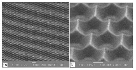
Figure 5: Scanning electron microscopy (SEM) image of the surface. (a) a perspective view of the texturizied surface (b) a plan view of the same structure. (Etched in the (HNO3:HF-50:1) solution).
The efficiency of a solar cell strongly depends on the interaction between the incoming light beam and the surface of the device. Any process enhances light-surface interaction increases absorption probability of the light; thus, improves generated current, in turn. Generated current could be improved either by light trapping or by increased device thickness. Considering fabrication costs and recombination losses, mechanically thin optically thick wafers are being focused on in terms of light trapping properties. Surface texturing among the other methods is an effective and more lasting technique in reducing reflections and improving light trapping.
Fabricated solar cells with different patterns ended up with different device performance. Amongst them, holes of 4 μm diameter and 5 μm gap showed a remarkable trend for varying hole depths. As plotted in Figure 6, increasing hole depth resulted in better cell performance [17,18].
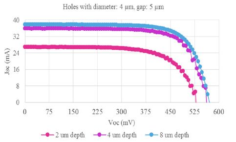
Figure 6: Jsc (mA) versus Voc (mV) comparison of surfaces having holes with diameter: 4 μm, gap: 5 μm, and depth: 2-4-8 μm.
Wet Acidic Texturing
Yerokhov et al. [19] developed a mathematical model of the macroporous silicon of the real layer with the multidimensional and multilayers macroporous crater-like surface for the cost-effective solar cells, which is easily possible to realize by chemical and electrochemical etching as shown in Figure 7.
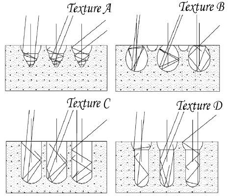
Figure 7: Possibility of texture formation on silicon surfaces by macroporus silicon layers using different geometrical models. In every figure, one can find three light ways to a texture body (10°, 30°, 45°).
Ju et al. [20] investigated a vapor texturing method, which has several advantages such as avoiding the step formation between grains, damage removal and texturing, relatively small etching depth (nano-scale) and aesthetically pleasing uniform appearance of the fabricated solar cells.
Initially, the wafers were cleaned by immersing them in an ultrasonic bath containing 3 wt% HCl and deionized (DI) water in the ratio 1:10 at 23°C for 3 min, which produces uniform surface cleaning.
Both saw damage removal and acid texturing achieved in a single step with the saw damage removal with texturing (SDRWT) process by using acidic solution. The acidic etching solution contains HF:HNO3:CH3COOH:DI water in the ratio of 8:21:10:8. The precleaned wafers were immersed in the prepared acidic etchant, which is maintained at 26°C, which monitored using an anti-corrosive thermocouple during texturing. After 3 min, the wafers were removed from the texturing bath and completely immersed in the deionized (DI) water flow to stop the reaction, then, thoroughly rinsed thereafter. Subsequent to cleaning via DI water, the wafers were dried by a spinning method. The etching depth was calculated as 4 µm both sides of the wafers. A SEM picture of the SDRWT surface using acidic solution is shown in Figure 8.
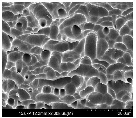
Figure 8: SEM picture of mc-Si wafer surface after acid texturing (SDRWT).
The SDRWT processed mc-Siwafers in a teflon holder was placed over the container with an optimized mixture of HF:HNO3 in the ratio 7:3. Then, the vapor was generated by adding 8 g of silicon to the HF:HNO3 mixture. The volume of HF:HNO3 used for the present investigation is 200 ml. The schematic of the vapor texturing setup is shown in Figure 9.
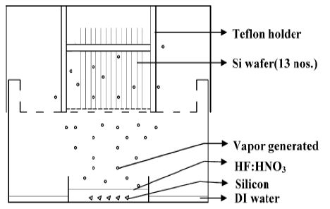
Figure 9: Schematic representation of the vapor texturing setup.
Uniform and homogeneous surface texturization was obtained in mc-Si wafers by the vapor texturing method, and it is also suitable for very thin wafers, due to minimal loss of material. The reflectance is about 6.5%. The reduction in reflectance can be explained by the roughness of the surface after nano-scale porous formation, which is shown in Figure 10, and the higher magnification is shown inside (nano-scale porous surface with pore size less than 50 nm). The improvement in the reflectance spectra with the nano-scale porous layer is due to interference effects in the layer, which implies that the nano-scale porous layer has different optical properties compared to the bulk mc-Si.
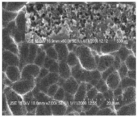
Figure 10: Nano-scale porous formation after vapor texturing (inside higher magnification).
Texturing the surfaces of silicon wafer is one of the most important ways of increasing their efficiencies. The texturing process reduces the surface reflection loss through photon trapping, thereby increasing the short circuit current of the solar cell. To date, the texturing of crystalline silicon is usually carried out using alkaline solutions. Such solutions resulted in anisotropic etching that leads to the formation of random pyramids. Before the texturing process is carried out, saw-damage etching is performed in order to remove the surface defects and damage caused by wire sawing. In general, potassium hydroxide (KOH) solution is used for saw-damage etching. This etching results in a fairly flat surface.
There are two major losses that reduce the conversion efficiency of silicon solar cells: optical losses and electrical losses. Optical loss by surface reflection can be prevented by the use of an anti-reflection coating or by surface texturing. It is well known that polished wafers reflect 30% of the incident light. By contrast, textured surfaces and anti-reflection-coated surfaces reflect only 10% and 3% of the incident light, respectively. Reducing the extent of surface reflection can increase the short circuit current and thereby increase the conversion efficiency of the solar cell.
Alkali hydroxide etchants, such as potassium hydroxide (KOH) and sodium hydroxide (NaOH), have been widely used to texture crystalline silicon solar cells. However, these days, simple and quaternary ammonium hydroxide etchants, typically tetramethyl ammonium hydroxide (TMAH) (firstly proposed by Tabata et al. in 1992 in order to make high-efficiency crystalline Si solar cells, the light reflection from the surface should be minimized and the formation of pyramidal surface of Si decreases the reflection substantially. To satisfy the requirement, alkaline-based anisotropic etchants (e.g. KOH, NaOH) have been widely used. However, as the alkaline-based solutions result in the mobile ion contamination to IC devices, a special effort has been made to develop new anisotropic etchants that do not introduce any mobile ions so that they can be IC fabrication compatible. Among these etchants, tetramethyl ammonium hydroxide (TMAH, (CH3)4NOH) solution shows full compatibility with IC technologies, nontoxic, and good anisotropic etching characteristics. Compared to alkaline-based etchants, TMAH is readily controllable and its etch rate is constant over long etch times [21]) TMAH are used instead of KOH and NaOH due to problems associated with metal ion contamination.
The major ion involved in the silicon etching process is the hydroxyl ion (OH–), which attacks the silicon surface:
Si + 2OH– → Si(OH)22+ + 4e–
Ions from the silicon crystal react with H2O in the solution. At the same time, the H2O dissociates and generates hydrogen gas:
4H2 + 4e– → 4H2O–
4H2O– → 4OH– + 2H2
The regenerated hydroxyl ions attack the neutral silicon again, thereby causing the reactions to continue.
Representative result of texturing for solar cell is forming random pyramids on the surface. Such pyramids are produced by anisotropic etching, which is caused by the difference in the densities of the planes in the (100) and (111) directions. Since the plane in the (111) direction is denser than that in the (100) direction, the etching rate in the (111) direction is much slower.
Isopropyl alcohol (IPA) is added in order to control the etching rate and thereby prevent an explosive reaction between the silicon surface and the OH– ions. In general, as-cleaned wafers or wafers that have been saw-damage etched using an alkaline etchant are used for the fabrication of solar cells. The random pyramids formed on these wafers are typically 7-10 mm in size. Acidic etching of silicon is isotropic in nature and therefore results in the surface features to become ‘‘round’’ in shape [22].
The mono-crystalline silicon wafers employed were boron-doped (100) wafers with resistivities 6-12 Ωcm. The thickness of wafers was 270 µm. The surfaces of the wafers were first cleaned in order to eliminate any organic and metal impurities. Both a sulfuric acid mixed with hydrogen peroxide solution (SPM) and a hydro chloric acid mixed with hydrogen peroxide solution (HPM) were used for this cleaning process, based on a standard RCA cleaning procedure [23]. After rinsing the wafers with sufficient de-ionized water (DIW) between each cleaning step, wafers were dipped in buffed oxide etching (BOE) solution in order to remove the native oxide layer. For comparison, wafers with three different surface morphologies were prepared.
Sample 1 was not saw-damage-etched wafer and Sample 2 was saw-damage etched with KOH solution. The final wafer was saw-damage etched with an aqueous acid mixture (Sample 3). All of the wafers were then anisotropically etched using solution mixture of KOH and IPA. The relevant chemical composition and process conditions are listed in Table 1.
Table 1: Chemical composition and process conditions.
| Process |
Chemical composition |
Temperature (°C) |
Time |
|
| Cleaning | SPM |
H2SO4:H2O2=2:1 |
80 |
10 min |
| HPM |
HCl:H2O2:DIW=1:2:5 |
85 |
10 min |
|
| Saw-damage etching | Sample 2 |
KOH |
80 |
10 min |
| Sample 3 |
HF:HNO3:CH3COOH=1:2:3+fluoric surfactant |
RT |
10-60 s |
|
| Texturing |
KOH:IPA:DIW=1:6:55 |
80 |
30 min |
|
The surface of Sample 1 just after cleaning was very rough and had many defects and damaged areas. When such defects and damaged areas are allowed to remain, it is difficult to fabricate uniform and well-aligned solar cell. Moreover, the efficiency of the solar cell was decreased by increased surface recombination probability of the electrons and holes. For these reasons, defects and damaged areas are removed by saw-damage etching, normally using an alkaline etchant. KOH was used (Sample 2). During the etching process, the wafers were isotropically etched at a rate of 2 mm/min against the (100) direction. The etching clearly reduces the surface roughness, as shown in Figure 11(b). Square shapes (10 mm width, 5 mm high in average) were formed on the surface during the etching process. As time progressed, the squares become wider, thereby flattening the surface.
However, when using an acidic solution (Sample 3) to remove saw-damages, it remained round in shape on the surface as shown in Figures 11c-11f. The mechanism of acidic saw-damage etching is shown below.
Oxidation 3Si + 4HNO3 → 3SiO2 + 4NO + 2H2O
Removing Oxide 3SiO2 + 18HF → 3H2SiF6 + 6H2O
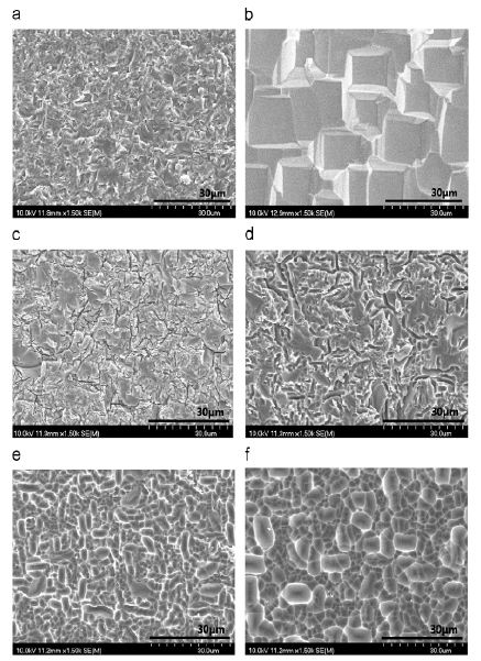
Figure 11: SEM images of the silicon surface: (a) as-cleaned wafer (Sample 1), (b) saw-damage-etched wafer using an alkaline solution (Sample 2), (c) saw-damage-etched wafer using an acidic solution (Sample 3) for 10 s, (d) for 20 s, (e) for 30 s, and (f) for 60 s.
First, silicon oxidation occurs upon exposure to nitric acid. Then, hydro fluoric acid removes the oxidized layer, thereby forms H2SiF6. At the same time, acetic acid acts as a buffering agent that prevents nitric acid from decomposing intoNO3– or NO2–.
In general, the etching time is a combination of the chemical reaction time and the transport time by diffusion. The process limitation is determined by the slowest time. In such case, the diffusion time is longer than the reaction time. In a transport-limited process like this, the etching selectivity is small and the surface is less important than in reaction-limited processes.
As a result, isotropic etching occurs. After etching, the surface is marked with round shapes. In the cross-sectional view, a wave-like surface was observed. The round crater-like features on the surface resulted from the conditions at the initial starting point of the etching process. Due to the relatively low concentration of HNO3, the reaction starts at sites of low activation energy (e.g., a surface defect) then diffuses into neighborhood sites. Therefore, as Figure 12 shows, the diameter of the round craters increases as time progresses.
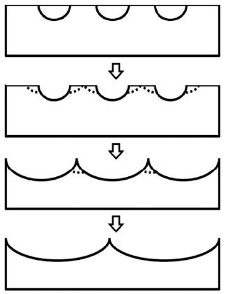
Figure 12: Schematic diagram of the silicon etching with an acidic etchant.
Upon texturing, using a solution of KOH in IPA, random pyramids were formed on all of different types of wafers. In the case of the just cleaned wafer (Sample 1), many defects remain on the surface after texturing (Figure 13(a)). However, Samples 2 and 3 do not show these defects due to saw-damage etching, as shown clearly from Figure 11. In order to define the size of the pyramids after texturing, intercept method was used. First, draw the diagonal line on the SEM image from Figure 13. As the scale bar indicates 50 mm, the length of line is 164 mm. Then count the number of pyramids caught by the diagonal lines. The length of diagonal line divided by number of pyramids gives the average value of pyramids size (Figure 14).
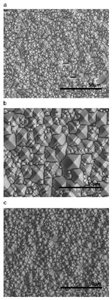
Figure 13: SEM images of the silicon surface after texturing with KOH+IPA mixture solution: (a) sample 1, (b) sample 2, and (c) sample 3 with 60 s etching.
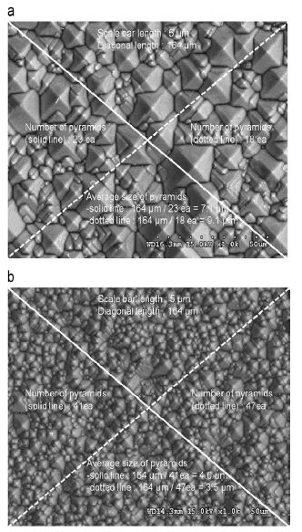
Figure 14: Intercept method using SEM image of Figure 13: (a) sample 2 and (b) sample 3.
The pyramids of Sample 2 were 7-10 mm in size. By comparison, the pyramids of Sample 3 were just 3-4 mm in size. These results show that the surface condition before the texturing step affects the formation of the pyramids.
When round craters on the surface are formed by acidic saw-damage etching, there could be more exposure of (111) planes that have lower etching rate due to high density of plane and resistivity. It seems to act as a stable starting point for etching. Hence, reducing the size of the pyramids means that more pyramids can form on the same surface area (Figure15).
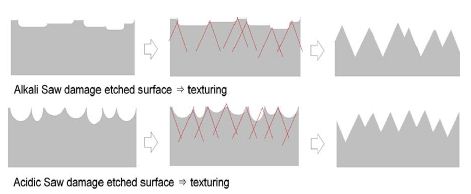
Figure 15: Schematic representation of the texturing process on different saw-damage-etched wafers.
Among the three solar cells, Sample 1 showed the lowest conversion efficiency. This can be caused by the many defects on its surface that increase series resistance. In contrast, Sample 3 showed the best cell characteristics. Compared to Sample 2, Sample 3 has a similar open circuit voltage (Voc) and fill factor (FF) but a higher short circuit current (Jsc) of about 3.4 mA/cm2. The increased Jsc indicates an improvement in the photo generation, as would be predicted from the lower reflectance observed in Figure 6. Therefore, this can explain that improved textured surface by acidic saw-damage etching contributes to enhance conversion efficiency by effective photon trapping evidenced by decreased reflectance and increased Jsc.
Chu et al. [24] proposed a simple and cost-effective approach for texturing crystalline silicon wafers without surfactant added in alkaline etchants.
The etching experiments were carried out using 300’’, p-type, <100>; oriented, crystalline silicon wafers with resistivity 1-3 Ωcm. Before texturization, the wafers were etched in 10% hydrofluoricacid (HF) to remove native oxide and rinsed in deionized water. The wafers were then etched in KOH (1 wt%) solutions at different temperatures for 10, 15, and 20 min. The etching solution was heated with a temperature-controlled hot plate. The hydrogen bubbles produced during etching were trapped on the wafer surfaces utilizing the stainless steel metal grids with different square openings with 1, 1.5, 2, and 3 mm square opening for texturing at 1 and 2 mm wafer-to-grid separations.
The pyramids fabricated using the proposed approach is dependent not only on the conditions of the KOH etchants but also on the structures of the metal grids to the silicon wafers.
Figure 16 shows the SEM photos of the surface morphology of the silicon wafers textured in the KOH solution at 90°C for20 min using the metal grids with different sizes of openings. The separation between the wafers and the grids was kept at 1 mm (Since the typical diameter of the bubbles was around 2-3 mm. Therefore, the bubbles could not function as the etch mask effectively during the etching. The bubble trapping capability of the grid decreased if the wafer and the grid were further separated.).
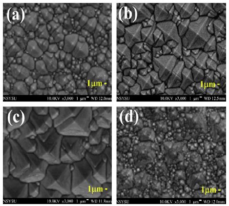
Figure 16: The SEM photos of the surface morphology of the silicon wafers textured in 1 wt% KOH solution at 90 °C for 20 min using metal grids with (a) 1, (b) 1.5, (c) 2, and (d) 3 mm2 openings.
Without any antireflection coating, an average weighted reflectance of 15.1% is achieved. In addition to the fact that isopropyl alcohol (IPA) was no longer needed in the etching process, the cost of the raw materials used throughout the entire texturization (buffered-HF pre-treatment, KOH-only texturing and HCl/buffered-HF/DI-water post-treatment) of the proposed approach is 0.105 USD/wafer, a considerable reduction if compared with the cost of 0.154 USD/wafer in the conventional texturing process.
Nowadays different technologies of crystalline silicon (c-Si) solar cells, consisting in mono, poly, and multi c-Si, represent nearly 80% of the total worldwide photovoltaic (PV) production.
For wet texturing solutions consisting of potassium hydroxide (KOH) or sodium hydroxide (NaOH), combined with deionized water (DI H2O) and isopropyl alcohol (IPA) were used to produce pyramid-like structures on c-Si surfaces with low reflectance values. SEM images of textured c-Si surfaces processed by different KOH/IPA/DI H2O based solutions listed in Table 2 are shown in Figure 17.
Table 2: Parameters of 6 different c-Si texturing processes using chemical solutions based on KOH/IPA/DI H2O.
|
Process |
KOH (wt%) | IPA (vol%) | Temperature (°C) | Time (min) |
| 1A | 1.5 | 3.8 | 70 |
30 |
|
1B |
1.5 | 3.8 | 70 | 50 |
| 2A | 1 | 8 | 80 |
30 |
|
2B |
1 | 8 | 80 | 50 |
| 3A | 1.35 | 7 | 70 |
30 |
|
3B |
1.35 | 7 | 70 |
50 |
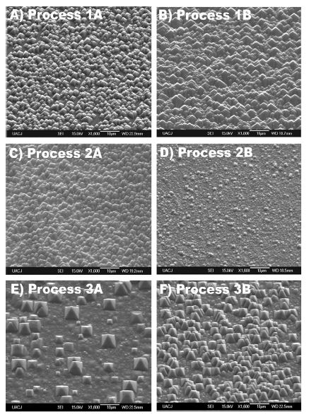
Figure 17: SEM images of textured c-Si surfaces processed by different KOH/IPA/DI H2O based solutions listed in Table 2.
For c-Si solar cells the tendency is to reduce the amount of silicon, since this represents the main cost of the overall solar cell, therefore one direction followed is the research of the development of ultrathin c-Si wafers.
On the other hand, there is a constant research on how to improve the c-Si solar cells fabrication processes, with the aim to increases the conversion efficiency, the study of light trapping in the silicon surface has attracted much attention, since a reduction in the amount of light reflected form the solar cell surface, results on an increase of the short circuit current (Isc) and therefore on the efficiency.
This issue has been partially solved using anti reflective coatings (ARC), as silicon oxide-SiO2 [Green 2003], silicon nitride-SiNx [25] and sol-gel Al doped zinc oxide-AZO [26], among others. Some of those films have demonstrated excellent optical transmittance (~90%) in the 400-1100 nm wavelength range. As well, for HIT solar cells, transparent conductive oxides (TCOs) as indium tin oxide-ITO are widely used due to their very high transmission values (close to 90% in the range of 300-900 nm of the electromagnetic spectrum) and low resistivity [27].
Another way to increase the conversion efficiency is texturing the c-Si wafer surface with alkaline solutions; this technique has been widely studied and incorporated to industry, since the pyramid-like structures that are produced are very suitable to reduce the reflected light to values below 15% [28].
Moreno et al. [29] used (100) CZ c-Si wafers of 10 cm2 and resistivity of 5-15 Ωcm for wet texturing processes; the KOH concentration was varied from 1 to 1.5 wt%, the IPA concentration was varied from 3.8 to 8 vol%, the temperature was in the range of 70-80°C, and two different times (30 and 50 min) were employed.
The diffused reflectance (R) as a function of the wavelength (in the range of 300-700 nm) of the textured samples using different KOH based solutions included as reference, the R value of a flat polished wafer, was tested. Results show that the average R of the reference wafer is 36%, while for samples 3A/3B is of above 27%. Larger reduction is observed in samples 1A, 2A and 2B with R of 18%, the sample 1B has the lowest value of R (13%).
Kim et al. [30] investigated how the wet chemical etching process to form random pyramids was affected by surface conditions.
The p-type (100) mono-crystalline silicon wafers with a resistivity of 0.5-3.0 Ωcm and thickness of 200 µm was used. To witness the texturing behavior, three different surface wafers were prepared, namely saw-damage etched (SDE), polished, and as-cut wafers.
Figure 18 shows scanning electron microscopy (SEM) images of the different surface conditions. The saw-damage etching process was performed with potassium hydroxide (KOH) for 10 min, at 80°C. The polished wafer was prepared by using chemical mechanical polishing (CMP). After preparing the different surface wafers, the texturing process was carried out using a 20 wt% tetra-methyl ammonium hydroxide (TMAH) solution with isopropyl alcohol (IPA) at 80°C. Analysis of the process was performed after 2, 5, 10, 20, 30, and 60 min.
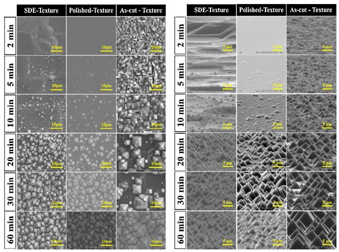
Figure 18: SEM images of textured surfaces over times 2, 5, 10, 20, 30, and 60 min for saw-damage etched, polished, and as-cut wafer samples; (a) surface and (b) tilted images.
The extent of the change in the morphology of the textured surfaces over texturing time is expressed in Figure 18. After 30 min of texturing time, the SDE sample is completely covered by pyramids. On the other hand, the as-cut and polished samples take more than 60 min to be covered. Surface texturing is an anisotropic wet-chemical etching technique that is commonly used to form random pyramids by utilizing differences in etching rates for the planes in the (1 0 0) and (1 1 1) direction. The saw-damage etching process carries out isotropic wet-chemical etching to eliminate micro-cracks caused by the use of a strong alkaline solution (e.g., KOH) for wire sawing. However, this process creates squares and inclined planes due to incomplete isotropic etching, as illustrated in Figure 19, where the inclined plane is rough with no flat character.
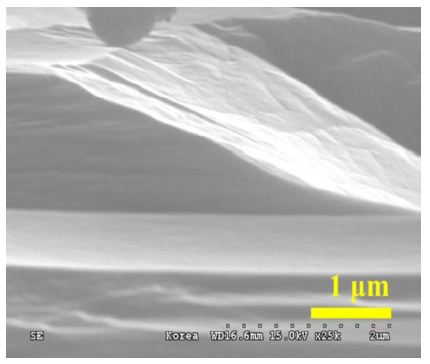
Figure 19: SEM images of an inclined plane after saw-damage etching to give a saw-damage etched wafer surface.
For the SDE sample, Figure 18(b) (2, 5, and 10 min) shows that pyramids are preferentially created in an inclined plane of squares that are generated through the saw-damage etching process. Because (1 1 1) planes are exposed by the inclined plane of squares, the SDE sample takes less texturing time than do the other sample types.
For the polished sample, pyramids are randomly created. The etching rate of the polished wafer is similar to any other defect-free surface; however, the as-cut sample was completely covered by secondary pyramids that were created after the first set of pyramids.
The etching reaction exhibited on the as-cut wafer is active due to the inherent surface defects, and for up to 10 min, many defects remain on the surface after texturing. After 20 min, the surface morphology does not indicate these defects, instead of the squares created by the saw-damage etching process since similar surface shapes were observed. During the texturing process of the as-cut wafer, texturing pyramids are created and surface defects are removed simultaneously.
As a result, texturing the surface of a silicon wafer brings about a reduction in the surface reflectance. The weighted reflectance of each sample is 11.0, 13.8, and 23.1% in SDE, polished, and as-cut wafer, respectively. However, each sample exhibits an almost equivalent reflectance after 60 min of texturing process time, where the reflectance is 10.7, 10.9, and 11.0%.
Lee et al. [31] proposed a process called electro-less etching to investigate the density and size of silicon nanowires on a pyramid-textured silicon surface and its photovoltaic performance, especially on the minority-carrier recombination lifetime of silicon nanowires, and photovoltaic performance on the density and size of silicon nanowires on the pyramid-textured silicon surface.
The as-cut (1 × 1 cm2) p-type silicon wafers with a resistivity of 1-3 Ωcm and a thickness of 200 µm were etched by using 2 wt% potassium hydroxide (KOH) solution to produce randomly distributed square-based pyramids on the silicon surface and to remove sawing damage. The pyramid-textured silicon wafers were dipped into the mixture solution of AgNO3 (0.068 g), deionized water (160 ml), and hydrofluoric acid (46 ml) for 30 s to deposit Ag nanoparticle masks on the pyramid-textured silicon surface. Then, the pyramid-textured silicon wafers with Ag nanoparticle masks were etched with a mixture solution of FeNO3 (8.16 g), hydrofluoric acid (HF: 46 ml), and deionized water (160 ml) for 0, 1, 2, 3, 4, 5, 7, 10, and 15 min, to produce silicon nanowires on the wafer surface.
The surface morphology of the pyramid-textured silicon surface as a function of the etching time of silicon nanowires is shown in Figure 20.
Selective alkaline etching using KOH produced uniformly distributed square-based silicon (111) pyramids, as shown in a cross-sectional and top view SEM image (inset, bottom left) in Figure 20a. Deposition of Ag nanoparticles using the mixture solution of AgNO3, deionized water, and hydrofluoric acid for 30 s followed by electro-less etching using the mixture solution of FeNO3, hydrofluoric acid, and deionized water for 1 min produced silicon nanowires 56 µm in diameter and 211 µm in height on the pyramid-textured silicon surface, as shown in the SEM, top view SEM image (inset, bottom left), and TEM image (inset, bottom right) in Figure 20b. The diameter of silicon nanowires on the pyramid-textured silicon surface increased initially up to ~56 nm when the electro-less etching time increased up to 2 min, and then maintained with ~109 nm although the electro-less etching increased further, as shown in Figure 20b-20i. Otherwise, the height of silicon nanowires on the pyramid-textured silicon surface increased from ~211 nm to ~1175 nm when the electro-less etching time increased from 1 min to 15 min, Figures 20b-20i. In particular, silicon nanowires tended to collapse with electro-less etching times that exceeded 10 min, as evident in Figures 20h and 20i.
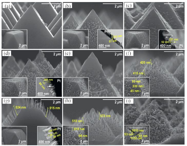
Figure 20: Surface morphology of silicon nanowires on pyramid-textured silicon surface depending on electro-less etching time: (a) 0, (b) 1 min, (c) 2 min, (d) 3 min, (e) 4 min, (f) 5 min, (g) 7 min, (h) 10 min, and (i) 15 min.
Results indicate that silicon nanowires on a pyramid-texture silicon surface probably enhance power conversion efficiency (PCE) by weakening the dependence of the light incident angle on PCE.
It illustrates that the silicon nanowire fabrication method using the Ag nanoparticle mask and electro-less etching is expected to be a key engineering technique that makes it possible to achieve maximum photovoltaic performance of silicon solar cells. Note that the p-type silicon photovoltaic cell with silicon nanowires on {111} pyramid-textured silicon surface enhanced ~10% in PCE compared to a conventional p-type silicon photo-voltaic cell that skipped anti-reflective coating process (plasma enhanced chemical vapor deposition). In addition, the process cost of the deposition of Ag nanoparticle mask and electro-less etching is probably similar or cheaper than that of anti-reflective coating process.
Srivastava et al. [32] reported a simple and fast etching process yet effective for nano-scale texturing of mc-Si surface using silver assisted wet chemical etching.
As-cut (1-2 Ωcm, B-doped) p-type mc-Si wafer of thickness ~250 µm and 100 × 100 mm2 size are used as the starting material. Samples of 50 mm diameter are diced from the large mc-silicon wafers in order to have the identical electrical/electronic properties. The samples are first cleaned and etched in an HNO3:HF:CH3COOH = 5:1:1 (v/v) etching solution to remove the saw damages. Thereafter, the samples are chemically polished (CP) in HF and HNO3 solution at ~4°C [33].
Three steps were taken: (i) deposition of a thin Ag layer onto the polished mc-Si using electro-less metal deposition in an aqueous 4 M HF solution containing 8 mM AgNO3 (for 10 s); (ii) etching of the Ag deposited samples in H2O:HF:H2O2::10:2:1 (v/v) solution at room temperature for 0-180 s; and (iii) removal of residual Ag particles from the samples in NH4OH + H2O2 solution. Finally, the mc-Si samples are rinsed in de-ionized water and blown dry with nitrogen.
The surface of the etched samples are black in appearance for etch duration; 20 s < tetch < 45 s; even under illumination at angles away from normal to the surfaces. For tetch > 45 s surface is brownish, as shown in Figure 21. The relevant detailed structures are shown in Figure 22. Results show that the nano-textured mc-Si surface with reflectance <5% enhances the photocurrent by ~20% in the short circuit current.
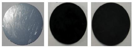
Figure 21: Optical images of mc-Si samples, ST (where the suffix, T = CP, 30, 60, 90, 120 and 180 represent polished, 30 s, 60 s, 90 s, 120 s and 180 s texturization time, respectively.)
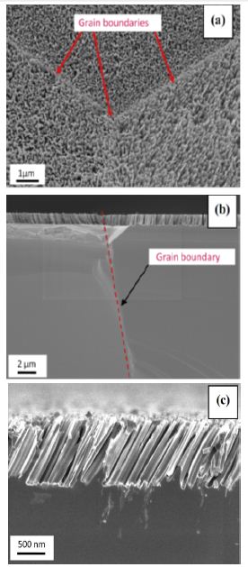
Figure 22: SEM images of a typical mc-Si surface (a) lateral view, (b) cross sectional view and (c) magnified cross sectional view showing nanotextured features formed at an angle (~30°) to the normal to the surface. Nano-textures are different in density and alignment with respect to the normal to the silicon surface. Grain boundaries are indicated by arrows in (a) and (b).
Future Prospects
Understanding the final wastes of wet acidic texturing is a critical issue to environmental pollutions. Unfortunately, it is still an area where a huge knowledge gap exists. The fate of final wastes and the resulting implications for environments-such as contaminated earth, pipelines, crops, under water, etc. are not well understood. The wider use of etchants in wet acidic texturing has increased their release into the environment through soil, water, and air, which may lead to unintended contamination of terrestrial and aquatic ecosystems.
The present state of knowledge in treatment with wastes of wet acidic texturing is still in a foundational stage along with silicon solar cell with nanostructures. Not only is data limited and inconclusive regarding texturing wastes’ and nano-silicon structures distributed in solar cells’ impacts in our daily life, but more information is needed on properties that control their effects in environments. Moreover, the interplay of these factors gives confounding results making it almost impossible to predict.
Therefore, the difference between the potential benefits and harm from wet acid texturing is quite subtle and a large knowledge gap exists on the long-term impacts to the environment, especially on the human health.
References
- Herche W (2017) Solar energy strategies in the U.S. utility market. Renewable and Sustainable Energy Reviews 77: 590-595.
- Kannan N, Vakeesan D (2016) Solar energy for future world: – A review. Renewable and Sustainable Energy Reviews 62: 1092-1105.
- Sampaio PGV, González MOA (2017) Photovoltaic solar energy: Conceptual framework. Renewable and Sustainable Energy Reviews 74: 590-601.
- Shah TR, Ali HM (2019) Applications of hybrid nanofluids in solar energy, practical limitations and challenges: A critical review. Solar Energy 1831: 173-203.
- Wolfe KD, Dervishogullari D, Passantino JM, Stachurski CD, Jennings GK, et al. (2020) Improving the stability of photosystem I-based bioelectrodes for solar energy conversion. Current Opinion in Electrochemistry 19: 27-34.
- Akbari H, Browne MC, Ortega A, Huang MJ, Hewitt NJ, Norton B, McCormack SJ (2019) Efficient energy storage technologies for photovoltaic systems. Solar Energy 192: 144-168.
- Hernández-Callejo L, Gallardo-Saavedra S, Alonso-Gómez V (2019) A review of photovoltaic systems: Design, operation and maintenance. Solar Energy 188: 426-440.
- Skoko SM, Ciric RM (2017) Laboratory exercises of photovoltaic systems-Review of the equipment, methodology, trials and results. Renewable and Sustainable Energy Reviews 79: 293-303.
- Heimsath A, Nitz P (2019) The effect of soiling on the reflectance of solar reflector materials – Model for prediction of incidence angle dependent reflectance and attenuation due to dust deposition. Solar Energy Materials and Solar Cells 195: 258-268.
- Yun MJ, Sim YH, Cha SI, Seo SH, Lee DY (2019) 3-Dimensional dye sensitized solar cell sub-module with oblique angled cell array for enhanced power and energy density output utilizing non-linear relation in cosine law of light incident angle. Solar Energy 177: 355-363.
- Bonilla RS, Jennison N, Clayton-Warwick D, Collett KA, Rands L, et al. (2016) Corona charge in SiO2: kinetics and surface passivation for high efficiency silicon solar cells. Energy Procedia 92: 326-335.
- Grant NE, Kho TC, Fong KC, Franklin E, McIntosh KR, et al. (2019) Anodic oxidations: Excellent process durability and surface passivation for high efficiency silicon solar cells. Solar Energy Materials and Solar Cells 203: 110155.
- Subramani T, Chen JY, Sun YL, Jevasuwan W, Fukata N (2017) High-efficiency silicon hybrid solar cells employing nanocrystalline Si quantum dots and Si nanotips for energy management. Nano Energy 35: 154-160.
- Tamang A, Sai H, Jovanov V, Bali SIH, Matsubara K, et al. (2016) On the interplay of interface morphology and microstructure of high-efficiency microcrystalline silicon solar cells. Solar Energy Materials and Solar Cells 151: 81-88.
- Manea E, Budianu E, Purica M, Cristea D, Cernica I, et al. (2005) Optimization of front surface texturing processes for high-efficiency silicon solar cells. Solar Energy Materials & Solar Cells 87: 423-431.
- Lindroos V, Tilli M, Lehto A, Motooka T (2010) Handbook of Silicon Based MEMS Materials and Technologies. Norwich, NY, William Andrew; Oxford: Elsevier Science.
- Altinoluk SH, Ciftpinar HE, Demircioglu O, Es F, Baytemir G, et al. (2016) Light trapping by micro and nano-hole texturing of single crystalline silicon solar cells. Energy Procedia 92: 291-296.
- Basu PK, Khanna A, Hameiri Z (2015) The effect of front pyramid heights on the efficiency of homogeneously textured inline-diffused screen-printed monocrystalline silicon wafer solar cells. Renewable Energy 78: 590-598.
- Yerokhov VY, Hezel R, Lipinski M, Ciach R, Nagel H, et al. (2002) Cost-effective methods of texturing for silicon solar cells. Solar Energy Materials & Solar Cells 72: 291-298.
- Ju M, Gunasekaran M, Kim K, Han K, Moon I, et al. (2008) A new vapor texturing method for multicrystalline silicon solar cell applications. Materials Science and Engineering B 153: 66-69.
- Tabata O, Asahi R, Funabashi H, Shimaoka K, Sugiyama S (1992) Anisotropic etching of silicon in TMAH solutions. Sensors and Actuators A: Physical 34: 51-57.
- Park H, Kwon S, Lee JS, Lim HJ, Yoon S, et al. (2009) Improvement on surface texturing of single crystalline silicon for solar cells by saw-damage etching using an acidic solution. Solar Energy Materials & Solar Cells 93: 1773-1778.
- Kern W (2018) Overview and Evolution of Silicon Wafer Cleaning Technology. Handbook of Semiconductor Water Cleaning Technology 3-85.
- Chu AK, Wang JS, Tsai ZY, Lee CK (2009) A simple and cost-effective approach for fabricating pyramids on crystalline silicon wafers. Solar Energy Materials & Solar Cells 93: 1276-1280.
- Duttagupta S, Ma FJ, Hoex B, Mueller T, Aberle AG (2012) Optimised antireflection coatings using silicon nitride on textured silicon surfaces based on measurements and multidimensional modelling. Energy Procedia 15: 78-83.
- Verma A, Khan F, Kumar D, Kar M, Chakravarty BC, et al. (2010) Sol-gel derived aluminum doped zinc oxide for application as anti-reflection coating in terrestrial silicon solar cells. Thin Solid Films 518: 2649-2653.
- Park YS, Kim E, Hong B, Lee J (2013) Characteristics of ITO films with oxygen plasma treatment for thin film solar cell applications. Materials Research Bullutin 48: 5115-5120.
- Leonard F (2012) Texturing, reflectivity, diffuse scattering and light trapping in silicon solar cells. Solar Energy 86: 319-325.
- Moreno M, Murias D, Martínez J, Reyes-Betanzo C, Torres A, et al. (2014) A comparative study of wet and dry texturing processes of c-Si wafers for the fabrication of solar cells. Solar Energy 101: 182-191.
- Kim H, Park S, Kang B, Kim S, Tark SJ, et al. (2013) Effect of texturing process involving saw-damage etching on crystalline silicon solar cells. Applied Surface Science 284: 133-137.
- Lee IJ, Paik U, Park JG (2013) Solar cell implemented with silicon nanowires on pyramid-texture silicon surface. Solar Energy 91: 256-262.
- Srivastava SK, Singh P, Yameen M, Prathap P, Rauthan CMS, et al. (2015) Antireflective ultra-fast nanoscale texturing for efficient multi-crystalline silicon solar cells. Solar Energy 115: 656-666.
- Green MA (2003) Crystalline and thin film silicon solar cells: state of the art and future potential. Solar Energy 74: 181-192.