Abstract
The application of nano materials, in developing a novel class of fiberoptic modulators, is presented. The developed modulators are capable of high speed modulation up to 140 Gbps. The technology is based on building the device directly on the surface of the optical fiber core in a cylindrical symmetrical and uniform fashion, for polarization independent and ultra high speed applications. The design of the device is based on modifying optical fibers by removing the fiber jacket and the passive cladding materials off a very short length of the fiber. Then, the fiber core, in the modified section, is coated with a multilayer structure of nano-materials. This modified cladding includes a nano layer of high-speed electro-optic polymer sandwiched between two nano metallic electrodes, for modulating signals application. In this way, the device speed can reach up to 140Gbps and more, based on the polymer’s improved electro-optic properties. Also, this structure can eliminates polarization dependent problems associated with all available integrated rectangular waveguide modulators. Which are used in most optical telecomm networks. Demonstration prototypes have been manufactured and successfully tested, and the proof of concept is completed.
OCIS Codes: Fiberoptic, Nano-materials, Optical modulators/switches, Optical communication, Optical networks, EO polymer, EO devices, Optical active devices, On-fiber devices.
http://www.photonicslabs.com;
http://www.photonicsonfiber.com;
https://www.linkedin.com/pub/dr-mahmoud-el-sherif/7/ab6/38b
Introduction
Because of the importance of integrated optics in optical communication networks, a great deal of effort has been expanded to take the advantage of newly developed nano materials to build Electro Optic (EO) devices directly onto the core of regular optical fibers, wherein, optical fibers can be used as active devices as well as the optical transmission link. In this way, many of existing problems associated with integrated optics can be eliminated, such as insertion loss associated with coupling optical signals between integrated optical devices and communication networks.
In this Letter, an overview on development of a novel class of fiberoptic modulators is presented. The development is based on using advances in nano materials in manufacturing active devices directly on the fiber core, in a symmetrical cylindrical and uniform structure. Also, this design eliminates polarization dependent in existing devices, which are constructed of rectangular waveguides acting as the device active channel. This technology can be applied to any ordinary optical fiber. So, the fiber can be used as an active device as well as the communication link, in any fiber network.
Most commercially available EO modulators are constructed of rectangular waveguides, made of Lithium Niobate (LiNbO3) crystals. They are polarization dependent devices. Therefore, the device has to be positioned next to the light source, or a polarization maintaining fiber has to be used between the light source and the device. Therefore, using this type of devices in any fiber network, imposes certain limitations on the device location with respect to the light source. Also, coupling light between the active channel of the device, which is a rectangular waveguide, and the circular cross section of the fiber core is another challenge.
In this Letter, a brief explanation of the developed technology is presented. The technology has been successfully tested in development of an EO modulator, and proof of concept has been completed. A demonstration prototypes have been manufactured and tested at low frequency. Results show perfect match between the modulating electric signals and the modulated optical signals, even when a triangle modulating signal was applied. The manufacturing of the devices is based on using novel processing techniques to have full control on the deposition thickness uniformity and parameters for each layers of the applied nano materials.
Available Technology
For more than three decades, much effort has been directed to the development of high-speed EO modulators for optical communication networks, using LiNbO3 rectangular waveguide as the device active channel [1,2]. The effort focused on improving the modulation efficiency as well as reducing insertion loss associated with those integrated devices. However, those modulators are polarization dependent, very costly and still have shown other drawbacks including coupling mismatch, and high insertion loss, when connected to fiberoptic networks.
On the other hand, the development of the high-speed EO polymers has resulted in a new generation of integrated EO modulators. The EO polymer is used as the active waveguide, to replace the single crystal LiNbO3 modulators. A lot of research has been done to improve the properties of the developed EO polymers as well as modulation efficiency [3–6]. However, because of the rectangular shape of the active channel, polarization dependent is still a problem. The rectangular structure of the active channel of this type of modulators has imposed so many limitations and disadvantages. The modulator has to be positioned next to the light source output, to limit the effect of polarization dependent. However, experimental research has proven that; even when the modulator is positioned near to the light source, the polarization dependent is still a problem. This is clear from the test results reported in reference [3], when the modulating signal is a triangle wave. It is shown that the modulated signal cannot follow the shape of the modulating signal. Instead of having a single peak as in the modulating triangle signal, a double peak is shown in the modulated signal, as shown in Figure 4 [3].
Based on polarization problems associated with integrated rectangular waveguide modulators, there were several reported trials with the intention of building passive and active devices directly on the fiber core. Passive devices were mainly built for various sensors applications. One of the main advantages, of using on-fiber structure for sensors applications, is to improve signal stability and accuracy, because of the device polarization independent [7].
For active on-fiber devices, challenges were not easy for coating very thin multilayers nano materials onto the cylindrical surface of the fiber core. Early trials were reported in 1980’s, before electro-optic polymers were developed or known. Also, it was impossible to grow or deposit electro-optic crystals, such as LiNbO3 crystal, on the cylindrical surface of the fiber core. Therefore, liquid crystals were used as the modified EO cladding [8, 9]. As a result, the problems of using rectangular waveguide were illuminated, however, using liquid crystal imposed sever limitation on the speed of the modulator.
Newly Developed Technology
Along with interest in solving the problems associated with those devices, a novel technology based on nano materials application, has been developed for manufacturing on-fiber modulators, as shown in Figure.1. This developed technology has resulted in a new class of polarization independent modulators. It is based on constructing a layer of nano EO material, as an active channel, sandwiched between two nano metallic electrodes directly on the cylindrical surface of the fiber core, in a cylindrical uniform structure. In his way, polarization dependent as well as coupling problems, exist between integrated devices and fiber networks, can be completely eliminated. This can be achieved by modifying a small section of ordinary optical fiber, replacing the passive cladding with an active multilayer cladding, using nano processing techniques. The multilayer modified cladding has to be surrounding the fiber core in a symmetric uniform 360o cylindrical shape. Also, in this way, there will be no need to cut the optical fiber to integrate optical modulators into the fiber network. The advantages of using this novel structure are unlimited, ranging from simplicity and cost effectiveness to high efficiency and high signal to noise ratio, as well as the devices are all polarization independent, because of the symmetrical uniform cylindrical structure.
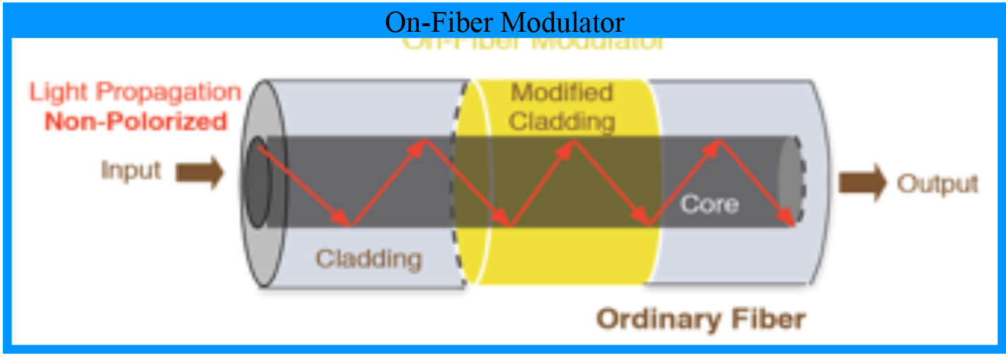
Figure 1. A schematic of an on-fiber EO Modulator, wherein, the device is constructed directly on the cylindrical surface of the fiber core.
Design and Manufacturing
In this Letter, an overview of the design, manufacturing and testing of the on-fiber EO modulator is presented. The design is based on modifying ordinary optical fibers in a small section, to act as an EO modulator. The fiber jacket is removed by mechanical stripping, then, the passive cladding material is partially (or totally) etched away, by a standard chemical etching technique. The etching process rate has to be calibrated, then, applied under continuous light transmission, for full control on the final thickness. This modified section is then prepared for multilayer coatings by applying the proper mask, before each layer of coating, based on the required geometry of this coating layer, as shown in Figure. 2 for the first layer of coating. The coating process is performed for each layer of the multi-layer structure, in 360o, as shown in Figure. 3. After each coating step the mask is removed and a new mask is applied based on the geometry of the next coating layer. The modified cladding includes a number of nano-layer of different materials. One of the layers is a high speed EO polymer, sensitive to electromagnetic fields. The polymer is coated by a spinning technique, used under certain conditions for nano layer coating. This layer of EO polymer is sandwiched between two cylindrical coated nano metallic electrodes, using enhanced plasma deposition technique. The inner electrode is deposited first, then, the polymer layer is coated, wherein, the poling process of the polymer is achieved in-situ using the first deposited electrode, under high voltage application in a high temperature oven. This process is applied for a certain time, under vacuum and nitrogen gas, to generate the electro-optic property within the coated polymer. Then, the second nano-metallic electrode is deposited on the top of the EO polymer. Before and after each of the coating steps a special surface treatment is performed. After the last layer of nano-materials is coated, the jacket material is applied on the top of the second electrode, as shown in Figure. 4.
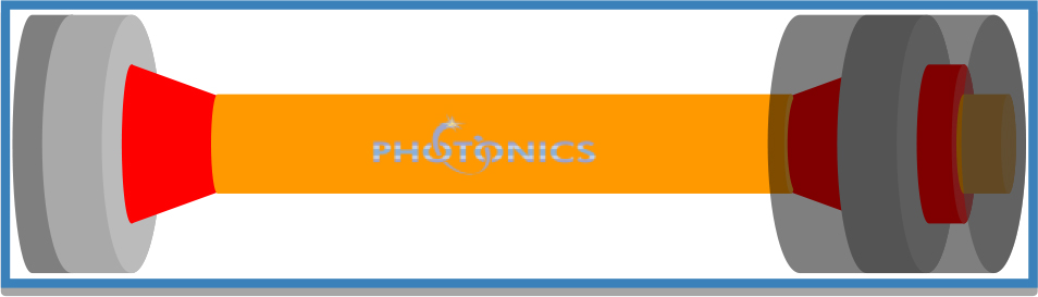
Figure 2. A schematic of the modified section of the optical fiber, after stripping the jacket and etching the cladding, and with the mask ready for the first coating process.

Figure 3. A schematic of the modified section of the optical fiber, after the multi-nano-layers coating, including the EO polymer and the two metallic electrodes.
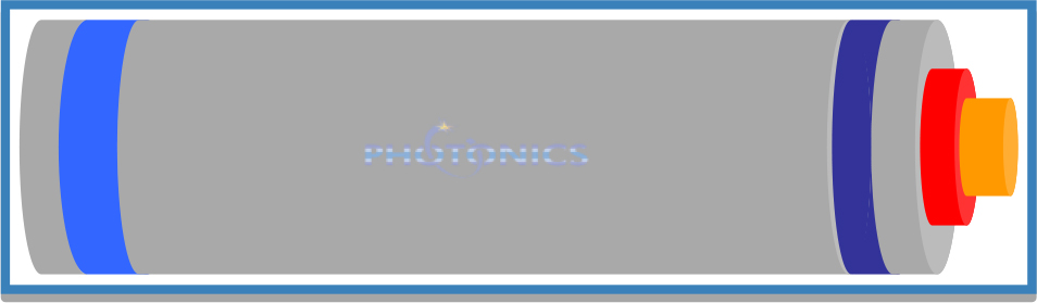
Figure 4. A schematic of the on-fiber EO modulator, after applying the jacket to the modified section, for handling and protection.
Several on-fiber EO modulators were manufactured and tested, based on the structural design explained before. For each modulator, after the passive cladding was etched away, the inner electrode was coated, in 360o, on the top of the fiber core, using a transparent nano metallic material, using an enhanced plasma deposition technique modified for cylindrical coating of fibers. Then, the polymer base material was spin coated on the top of the inner electrode, while it was synthesized. Adjusting the spin coating process, speed and time, controls the thickness of the coated thin layer of the polymer. After drying in a nitrogen oven at room temperature, the polymer was radially poled for about one hour at the required temperature and voltage, using the corona poling method. It was then cooled down to the room temperature while keeping the poling voltage on. The thermosetting cross-link of the material system occurred simultaneously during the poling process. This process is very critical to satisfy the required change in the polymer high speed electro-optic property. Detailed information concerning the synthesis process and the in-situ poling of the polymer are reported elsewhere [5].
After the coating process of the EO polymer is completed, the outer metallic electrode was coated on the top of the EO polymer. Before coating any of the electrodes or the EO polymer, special chemical surface treatment was conducted to enhance interface properties. Then, the jacket material was applied on the top of the second electrode. The design of the jacket includes two exposed metallic rings, which are connected to the electrodes. All coated layers were designed in a symmetrically uniform cylindrical structure, in 360o. The schematic of the manufactured EO modulator is shown in Figure. 4.
In the presence of a modulating signal, applied to the electrodes, an electromagnetic field is generated between the two electrodes resulting in changing the optical properties of the EO polymer, mainly the equivalent refractive index of the polymer material. This change will be uniform across the 360o of the cylindrical surface of the fiber core, resulting in a uniform modulation of optical signals propagating within the fiber core, regardless of the polarization direction of the propagating optical signals within the fiber core. Thus, the problem of polarization dependent, in commercially available devices, has been eliminated. Another major advantage is that; modulation can exist at more than one location along the length of the same optical fiber, and can be far from the light source location.
Several modulators were manufactured and successfully tested. Different types of modulating signals (sinusoidal, triangle, and digital) were used for testing the manufactured devices. Also, two different experimental test set-ups (Mach zehnder or Michelson interferometers) were used in testing and proof of concept. All test results were encouraging, and modulated signals were always identical to the modulating signals. One of testing results, of the manufactured devices, is presented next.
Testing Results
Before testing the selected device, a reasonable packaging process was done, using available tools and facilities. An actual image of the packaged device is shown in Figure. 5, which is in size about 1.0in x 2.0in x 0.3in. Using the proper packaging tools and facilities, the device size can be reduced by 80% or more, and it can also be in a cylindrical shape with a diameter less than 0.3in and length about 1.0in to 1.5in. The packaging process includes the integration of a RF/MW socket connected from inside with the two electrode rings. Also, for fiber mechanical protection, two rubber sleeves were used to cover the exposed fiber ends.
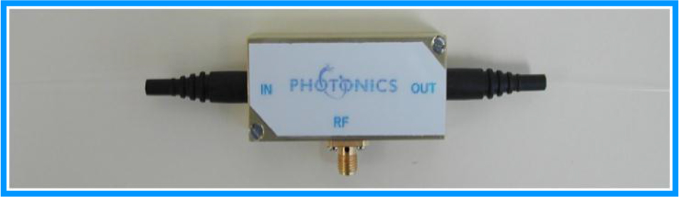
Figure 5. An actual image of the manufactured EO modulator, after packaging with a metallic shield box. The fiber two ends are exposed from both sides, and protected by two black rapper holder. The microwave socket is connect from inside with the two metallic rings on the fiber jacket, for direct application of the modulating signals.
A sample of the device test results is presented here, using the Michelson interferometer set-up. The schematic diagram of the Michelson test set-up is shown in Figure 6. The Figure shows two input signals to the oscilloscope. The inputs are the modulating electric signal and the photo-detector output, which is the modulated signal.
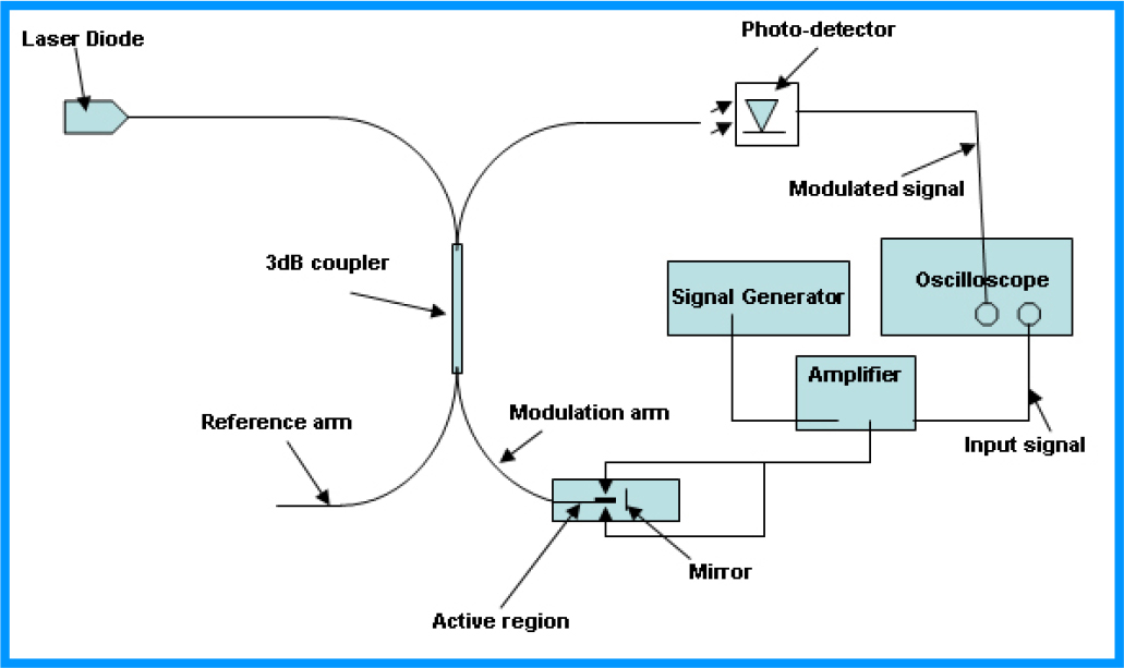
Figure 6. A schematic of a Michelson interferometer test set-up, used for the evaluation and proof of concept of the developed on-fiber EO modulator, showing the input signal (as modulating electric signal) and the photo-detector output (as the modulated signal).
A sample of the test result is shown in Figure. 7. It shows that the modulating signal is a triangle signal. This type of modulating signal was selected to proof the high quality polarization independent. It is clear from Figure. 7 that the modulated signal is following exactly the shape of modulating signal, with a triangle shape too. For better understanding of the achieved high quality performance of this on-fiber modulator, a comparison has to be done with respect to the modulated signal of a device consisting of a rectangular waveguide channel. This was explained before, using the results reported in reference [3], which explain that when a triangle’ modulating signal is applied to a rectangular waveguide modulator, a double peak signal will result at the device output, as a result of the device polarization dependent. This polarization dependent is clear, as presented in reference [3], even when the device is positioned next to the light source as in Figure. 4 of the reference [3]. On the other hand, this novel on-fiber modulator shows a smooth single peak in the modulated signal, even when the device is positioned far from the light source. Therefore, the polarization dependent has been completely eliminated. Based on recent advances in available EO polymers the device speed can now reach 140 Gpbs, and expecting much higher speed in the near future. Also, the developed technology can be applied to other type of devices, such as EO switch, tunable couplers and wave division multiplexers.
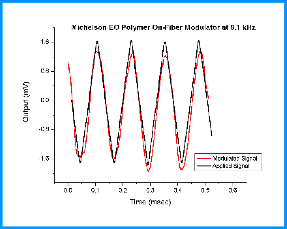
Figure 7. A sample of the test result showing a sawtooth (triangle) applied modulating signal and the photo-detector output of the modulated optical signal, using the Michelson interferometer setup in figure 6.
Conclusion
A novel class of on-fiber EO modulators has been developed, manufactured, and successfully tested, using advances in processing of nano-materials. The technology is based on building the device directly on the fiber core, after removing the fiber jacket and etching the cladding layer. For demonstration, an on-fiber modulator was manufactured, using a nano-layer of advance EO polymer as the active channel within the fiber modified cladding. The layer of the EO polymer was sandwiched between two uniform cylindrical electrodes. Ordinary optical fiber can be used for such application. The test results were encouraging and provide a clear proves on polarization independent. The device can be used for application up to 140Gbps, and can be constructed at any location on the optical fiber and fare from the light source. Multiple devices can also be constructed on the same fiber at different locations. The developed on-fiber technology can be used for the actual realization of all-fiber networks, where the fiber is used as an active device as well as the networking link. In addition, the technology has been tested in application to on-fiber switches, tunable couplers and tunable DWDM.
The author gratefully acknowledges that the EO polymer used in most developed and tested modulators were provided by Prof. Alex Jen and his group, including Dr. Antao Chen, and Dr. Jingdong Luo, of the University Of Washington, USA.
References
- Ed L. Wooten, Karl M. Kissa, Alfredo Yi-Yan, Edmond J. Murphy, Donald A. Lafaw, et al. (2000) A Review of Lithium Niobate Modulators for Fiber-Optic Communications Systems. IEEE J. of Selected Topics in Quantum Electronics 6: 69–82.
- High-Speed Photonic Devices, Edited by Nadir Dagli, CRC Press, Taylor & Francis Group, 2007
- Dechang An, Zan Shi, Lin Sun, John M. Taboada, Qingjun Zhou, et al. (2000) Polymeric electro-optic modulator based on 1Ã2 Y-fed directional coupler. Appl. Phys. Lett 76: 1972–1974.
- Dechang An, Suning Tang, Zu Zhou Yue, John Taboada, Lin Sun, et al. (1999) Linearized Y-coupler Modulator Based on Domain-inverted Polymeric Waveguide. SPIE Conference on Optoelectronic Interconnects VI, San Jose, California, SPIE, 3632: 220–231.
- Ma H, Jen AK-Y, Dalton LR (2002) Polymer-based optical waveguides: Materials, processing, and devices Advanced Materials 14: 1339–1365.
- Taylor EW, Nichter JE, Nash FD, F. Haas, Szep AA, et al. (2005) Radiation resistance of electro-optic polymer-based modulators Appl. Phys. Lett 86: 201122-1–201122-3.
- Optical Guided-wave Chemical and Biosensors II, Chapter 5: Fiber Optic Chemical and Biosensors, Mahmoud El-Sherif, Editors M. Zourob and A. Lakhtakia, Springer-Verlag GmbH, Germany (2010)
- El-Sherif MA, Shankar PM, Herczfeld PR, Bobb L, Krumboltz H (1986) On-Fiber Electro-optic Modulator/Switch. Appl. Opt 25: 2469–2470.
- El-Sherif MA, Shankar PM, Herczfeld PR, Bobb L, Krumboltz H (1987) An on-fiber active transducer in Technical Digest, IEEE Fourth International Conference on Solid-State Sensors and Actuators, 200–203.