Abstract
The rapid integration of VLSI circuit is due to the increased use of portable wireless systems with low power budget and microprocessors with higher speed. To achieve high speed and lower power consumption, the fabrication technology and power supply must be scaled down simultaneously. In this article, the digital circuits with low power, high speed and small size was designed with different method. The major goal of this paper is to design and implement of digital comparator using different logic techniques and compared in terms of different electric parameters. The results are simulated on the tanner-EDA tool realized in 90-nanometer technology at 1.3v supply voltage.
Keywords
Digital Comparator, Transmission Gate Logic Technique, Half Adder Logic Technique, Power Dissipation, Propagation Delay
Introduction
As the demand for higher performance CMOS VLSI processors is increasingly complicated, we need to improve the performance, area efficiency, and functionality of arithmetic circuits [1]. One of the challenges in VLSI processor design today is to structure low power digital comparator [2-3] circuits specifically for the 8-bit digital comparator circuits without limiting the functional flexibility. The major tradeoff of these prior gigahertz logic circuits is the high power consumption due to the unavoidable power consumption even in a standby condition, which is not a tolerable price to pay in recent mobile technologies. Since the usage of the digital comparator principle for high speed arithmetic units remains dominant, much effort has been focused on the improvement of low power digital comparator design [4]. A low power high performance circuit technique has been proposed previously [5] for reducing power dissipation and diminishing propagation delay by feeding through dynamic CMOS logic structure. In this paper, digital comparator is designed using different techniques with the low power consumption and higher packing densities in 90-nanometer technology at 1.3v supply voltage.
Two-bit digital comparator
The traditional method in digital logic of two variable A (A0, A1) and B (B0, B1) of a two-bit binary number is a logical operation that figures out whether A is less than B, A is greater than B and A equal to B [6-7]. Therefore, the digital comparator is such type of logic circuit that thinks about the relative magnitudes of these two variables. The block diagram of digital comparator appears in Figure 1. The result of digital comparator is determined by three variables that demonstrate whether A>B, A<B, or A=B. These also described by their logic function as
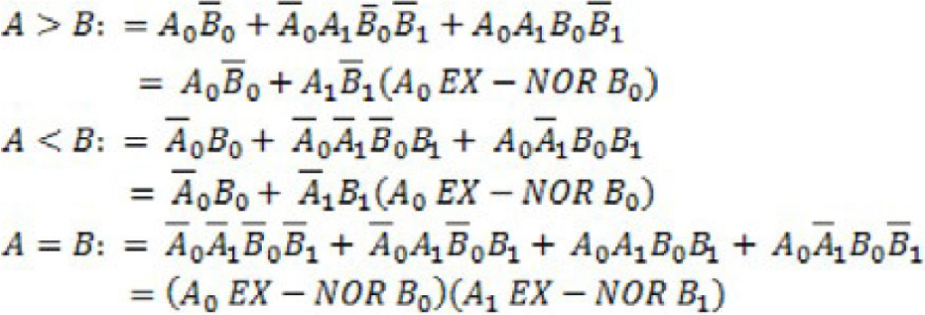
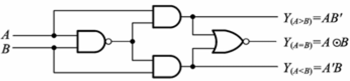
Figure 1. Block diagram of digital comparator.
The gate implementation of a two-bit digital comparator appears in Figure 2.
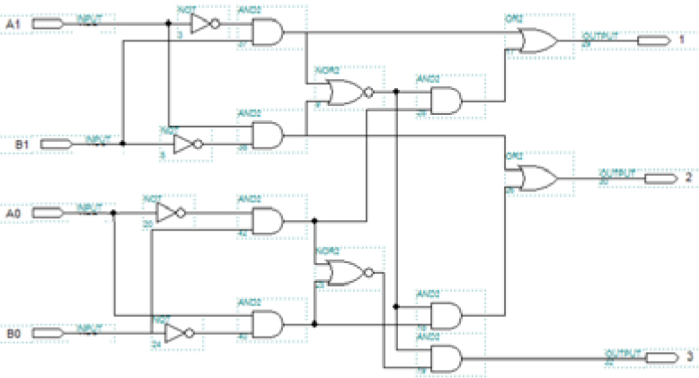
Figure 2. Gate implementation of a two-bit digital comparator.
Two-bit digital comparator design using cmos logic style
Since CMOS consumes less power and provides high speed, therefore it is considered as the best alternative design process in the digital circuit. The CMOS circuit consists of two networks, one NMOS pull-down network, which connects the output to the ground and another PMOS pull-up network, which connects the output to supply, as shown in Figure 3. The two-bit digital comparator using the CMOS logic technique is shown in Figure 4[8].
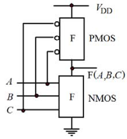
Figure 3. CMOS logic techniques.
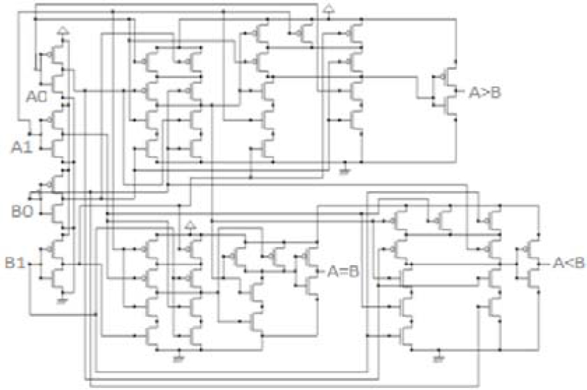
Figure 4. Two-bit digital comparator using the CMOS logic technique.
Two-bit digital comparator using the transmission gate logic style
The transmission gate logic gives high speed and less power dissipation than conventional CMOS for the reason that of the small transistor stack height, the least number of transistors and no complementary input signals are required. The transmission gate comprises of one NMOS and one PMOS transistor, which are associated in parallel. The graphical symbol of the transmission gate appears in Figure 5.
However, the existing transmission gate logic based two-bit magnitude comparator is shown in Figure 6 which consists of 66 transistors [9]. The large number of transistors, the more power consumption and lower packing density.
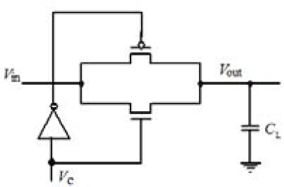
Figure 5. Graphical symbol of the transmission gate.
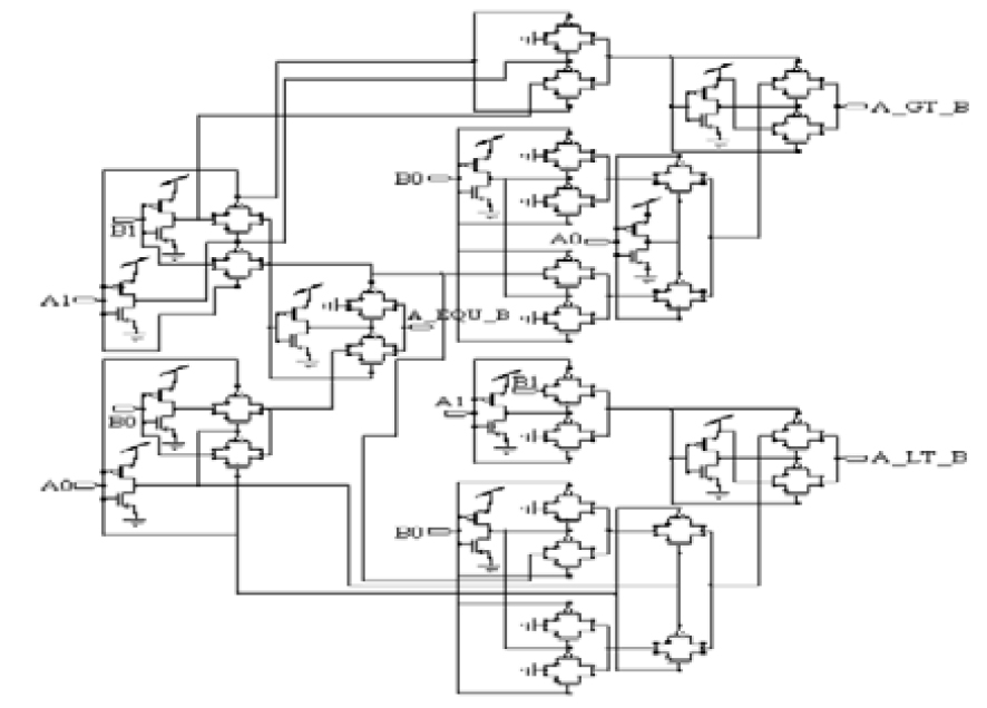
Figure 6. Schematic of the existing two-bit digital comparator using the transmission gate logic.
The proposed two-bit digital comparator using gdi gate and half adder logic style
In order to decries the transistor number of circuits, we are proposed two-bit comparator with transmission gate logic and half adder logic with 19 and 20 transistors, respectively, as shown in
Figure 7 and Figure 8.
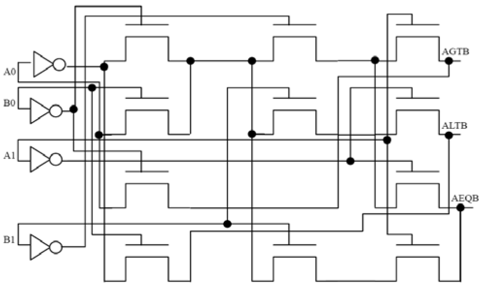
Figure 7. Schematic of the two-bit digital comparator using transmission gate logic technique.
In this proposed designed technique a digital comparator has been designed using half adder and basic logic gates. Implementation of the design procedure using hardware requires two sub-block one is half adder block and another is GDI gate comparison block.
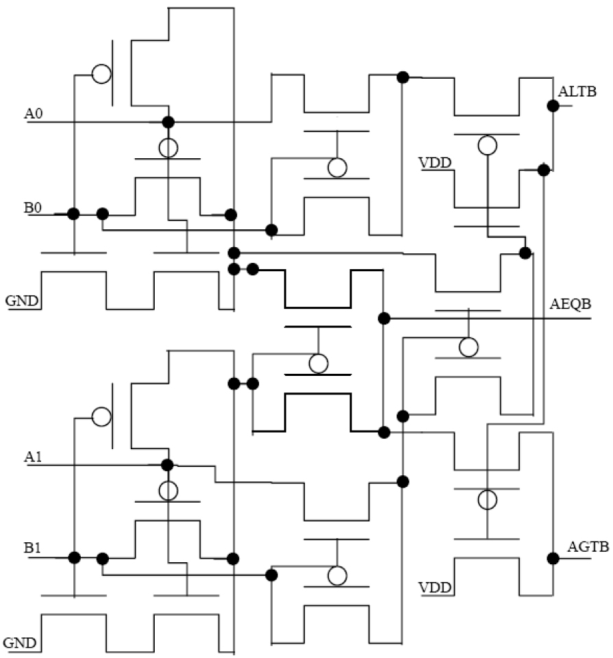
Figure 8. Two-bit digital comparator based GDI AND/OR gate and half adder logic technique.
Simulation results
The simulation result is measured by the EDA Tanner tool in 90 nanometer technology using various inputs A0=110011, A1= 001111; B0=111100, B1= 001111 at 1.3v supply voltage. The Layout(portion) design and wafer fabrication(SEM photo) of the proposed two-bit digital comparator using half adder logic is shown in Figure 9. The power consumption of this half adder logic based 2-bit digital comparator is 0.12 microwatt. The simulation result is listed in Table 1.
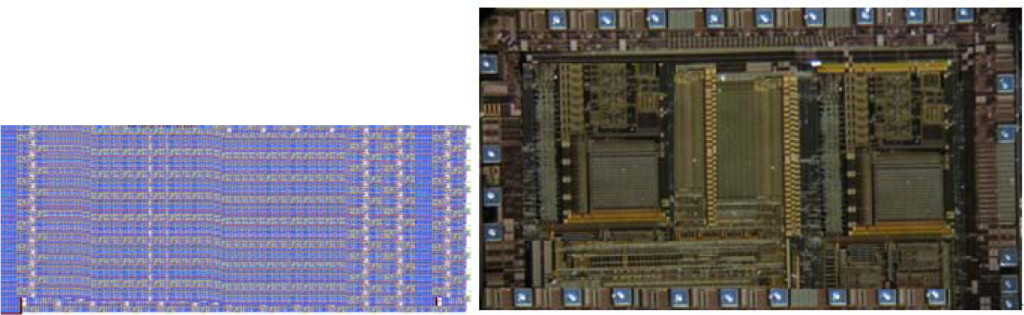
Figure 9. Layout(portion) design and wafer fabrication(SEM photo) of the optimized half adder logic based two-bit digital comparator.
Table 1. Performance comparison of two-bit digital comparator
|
Parameters |
Conventional |
Transmission Gate logic [9] |
Proposed Transmission Gate logic |
Proposed Half adder logic |
| Number of transistor | 54 | 74 | 19 | 20 |
| Power consumption (μW) | 0.62 | 0.47 | 0.28 | 0.12 |
| Propagation delay (n-sec) | 8.39 | 8.47 | 7.59 | 6.74 |
| Power delay Product(μ-nJ) | 5.19 | 3.87 | 2.12 | 0.79 |
Conclusions
Our proposed two bit digital comparator with modified transmission gate logic and half adder logic which verified with condition of on 90-nanometer technology at 1.3v supply voltage based on the tanner-EDA tool. After consider of all kinds of outline strategies, the simulation results are gotten for Power Consumption, Delay and Power Delay Product. Power consumption of the proposed half adder logic based two bit digital comparator is 1.12μW which is almost 65.83% less than existing transmission gate logic based two-bit digital comparator[9]. Also the transistor count of our proposed transmission gate logic circuit is almost 69.69% less than existing transmission gate logic based two-bit digital comparator, subsequently our chip area overall is minimized.
Funding
This research is supported partly by the National Natural Science Fund Committee of China (NSFC) (no.51377025, 20171BAB202037)
References
- Kang and Y. Leblebici : CMOS Digital Integrated Circuit, Analysis and Design (Tata McGraw-Hill, 3rd Ed, 2003). 295–302.
- Bellaouar and Mohamed I. Elmasry, Low Power Digital VLSI Design: Circuits and Systems (Kluwer Academic Publishers, 2nd Ed, 1995).
- Kathirvelu, T.Manigandan, ‘Design and Implementation of High speed ALU using Optimized PDP adder and Multiplier’, Journal of Applied Sciences Research, 8(4) (2012) 2100–2108.
- Victor Navarro-Botello and Juan A. Montiel-Nelson, Saeid Nooshabadi and Mike Dyer, ‘Low Power Arithmetic Circuits in Feedthrough Dynamic CMOS Logic’, MWSCAS ‘06. 49th IEEE International Midwest Symposium on Circuits and Systems, 1 (2006) 709–712.
- Saeid Nooshabadi, and Juan A. Montiel-Nelson, ‘Fast Feedthrough Logic: A High Performance Logic Family for GaAs, IEEE Trans. on Circuits and Systems-I: Regular papers, 51(11) (2004) 2189–2203.
- Mariano Aguirre-Hernandez and Monico Linares-Aranda, CMOS Full–Adders for Energy-Efficient Arithmetic Applications, IEEE Transaction on Very Large Scale Integration (VLSI) System, Vol. 19, no. 4, pp. 718–721, April. 2011.
- Wairya, R. Kumar Nagaria, and S. Tiwari, Compartive performance analysis of XOR-XNOR function based high peed CMOS full adder circuits for low voltage VLSI design, International Journal of VLSI Design & Communication Systems(VLSICS), Vol.3,no.2,pp.221-242, Apr. 2012.
- Mukherjee D. N., Panda S., Maji B., OPTIMIZATION OF DIGITAL COMPARATOR USING TRANSMISSION GATE LOGIC STYLE, International Journal of Advanced Research in Engineering and Technology (IJARET), Volume 7, Issue 4, July-August 2016, pp. 06–16
- Anjuli, Satyajit Anand, two-bit Magnitude Comparator Design Using Different Logic Styles, International Journal of Engineering Science Invention, ISSN (Online): 2319 – 6734, ISSN (Print): 2319 – 6726 www.ijesi.org Volume 2 Issue 1 PP.13–24, January. 2013.