Abstract
The electrochemical deposition of In2S3 thin films was carried out from an aqueous solution of InCl3 and Na2S2O3. The effect of the potential of deposition was studied on the cell parameters of CZS based solar cells. The obtained films depending on the deposition potential and thickness exhibited complete substrate coverage. Maximum photoelectric conversion efficiency of 12.0% was obtained, limited mainly by a low fill factor (65%). Further process optimization is expected to lead to efficiencies comparable to CdZnS buffer layers.
Keywords
Indium sulfide; CZS solar cells; Electrodeposition
Introduction
Solar cells based on CdZnS (CZS) chalcopyrite absorbers have reached 20.0% conversion efficiencies at the laboratory scale, using high vacuum processes. However, due to the toxicity of cadmium and the possible gain in current associated with the use of a wider bandgap material, many works are carried out with the aim of developing alternative buffer layers. The In2S3-based material is among the most relevant alternatives. Several techniques, such as sputtering, atomic layer deposition (ALD), evaporation and chemical bath deposition (CBD) have been used to synthesize In2S3 thin films on CZS. However, it seems that soft chemical based deposition techniques such as CBD which do not damage the surface of the absorbers and can provide highly conformal coating are more suitable to get high efficiency Cd-free CZS solar cells. Electrodeposition is a soft technique widely used in industrial processes for large area coating, both in batch and inline systems. This method, more recently applied to semi-conductor synthesis, may allow to control the width of the bandgap and the doping level by monitoring solution composition, applied potential, pH and temperature. Moreover it provides conformal growth with controlled thickness layers. All these advantages yield the method attractive for the synthesis of the absorber, the buffer layers as well as the transparent conductive oxide layer in CIGSe-based solar cells. Even if important works have been done on the electrodeposition of the CZS-based absorbers, very few attempts have been carried out so far to electrodeposit In2S3 buffer layers [1-7].
Experimental Section
The electrodeposition of In-S based layers was carried out using an aqueous solution containing indium chloride (5 mM), sodium thiosulfate (20 mM) as sulfur source and potassium chloride as supporting electrolyte (0.1M). A standard three-electrode setup was used. The reference electrode was a saturated mercurous sulfate electrode (MSE, E°=0.64V/NHE) and platinum was used as the counter electrode. The deposition was carried out at 60°C. A preliminary investigation was carried out on molybdenum-coated glass substrates to determine the optimal deposition conditions. In-S layers were then deposited on CdZnS absorbers, Al and glass substrate provided by Würth Solar. The surface morphology of the samples was investigated by scanning electron microscopy (SEM) using a Leo Supra 35 field emission gun (FEG). The electrical properties of cells were characterized by current voltage measurements at 25°C under illumination (AM1.5 global spectrum). Absolute spectral response measurements were made with a monochromator under chopped illumination and a lock-in technique. Thermal annealing at 300°C for 10 min in air and light soaking for 60 minutes under AM 1.5 solar-type spectrum were typical post treatments.
Results and Discussion
In order to define the optimal deposition potential range of the In-S thin films and the role of S, a voltammetric investigation was carried out both on Al and ITO glass substrates. Figure 1 shows cyclic voltammograms recorded at 60°C on Al and CZS substrates. As is observed on this figure, on both substrates, the deposition starts at potentials lower than -0.8V/MSE. the deposition process is more significantly inhibited on CZS absorber. On CZS a plateau is observed corresponding to a low current density between -0.8 and -1.2V, which might indicate that a different nucleation and/or deposition process occurs on this substrate compared to Al.
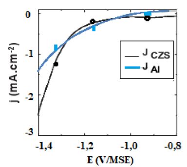
Figure 1: Voltammetric curves recorded at 5 mVs-1, 60°C. for 0.1 M KCl, 5 mM InCl3 and 20 mM Na2S2O3 solution on Al and CZS substrates.
When sodium thiosulfate is added to the In(III) solution, a whitish colloid solution is formed. This is due to the formation of elemental sulfur which is favoured at low pH values where the Na2S2O3 is decomposed. For solutions with the mixture of sodium thiosulfate and In(III), no oxidation peak of the In-S layer on the reverse scan is observed, whatever the substrate used, indicating the formation of a passive layer during the oxidation process. Based on these observations, when InCl3 and Na2S2O3 are mixed in acidic solutions and for potential lower than – 0.9 V/MSE, In-S compound can be formed, thanks to In2S3 energy formation (DG°=-420 kJ mol-1). In-S layers were deposited at various potentials on Al and CZS substrates for different electrical charges between -1.0 and -1.3 V/MSE under potentiostatic conditions. The evolution of the film morphology is presented in Figure 2. SEM observations point out that the substrate nature has a marked influence on the morphology of the buffer layer.
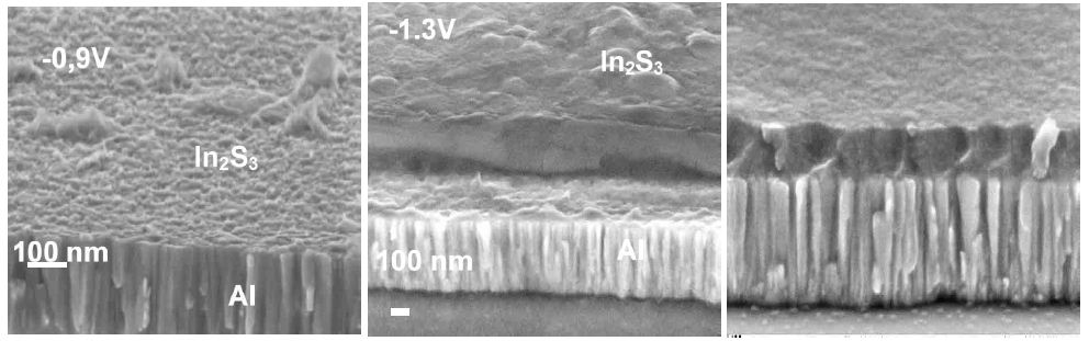
Figure 2: Effect of the potential of deposition on film morphology deposited on Al substrate The thickness of In2S3 on Al as function of potential are: -0,9 V: 16.5 nm, -1.1 V: 124 nm and -1.3 V: 178 nm.
For films deposited on an Al substrate (Figure 2 upper part) we can observe that, whatever the potential of deposition, films remain dense and homogenous and for the same deposition time, the electrical charge and the thickness of the buffer layer increase by decreasing the potential of deposition from -1.0V, to -1.3 V/MSE.
In parallel, In2S3 deposited films on CZS absorbers are dense, homogenous, and provide a conformal covering of the absorbers for films deposited at low potential <-1.1 V/MSE. However, as soon as the potential and the thickness of the layer increases, a transition in the morphology is observed and more or less disordered nanorods are growing (Figure 2).
The global film stoichiometry can be estimated by correcting the total O % measured from a C/4 quantity corresponding to a classical ratio of O involved in the carbonaceous contaminant layer. The In/(S+O-C/4) ratios obtained are close to 0.7 for deposition at -1.3 V and -1.2 V and close to 1.0 when proceeding at -1.0 V. These values approach the one expected for an In2SxOy compound (with x+y=3), which is 0.66. This means that in our case, we probably do not deposit a pure In2S3 layer but a mixture of oxide, hydroxide and/or oxi-sulfide compound (In(S, O, OH)). Such a mixed structure was already observed for In2S3 buffer layers deposited by electrodpeosition. More studies are in progress to have a better understanding of the evolution of composition of our films. Cells with electrodeposited In2S3 layer at different deposition potentials were prepared using co-evaporated CZS absorbers. Finally, a post annealing of the completed cells in air at 200°C for 10 min and a light-soaking at room temperature for 1 h were made. Figure 3 shows the dependence of the efficiency of the CZS cells with In-S buffer layers prepared at different potential (-0.9V, -1.1V, -1.3V) and different electrical charges used for the buffer layer deposition.
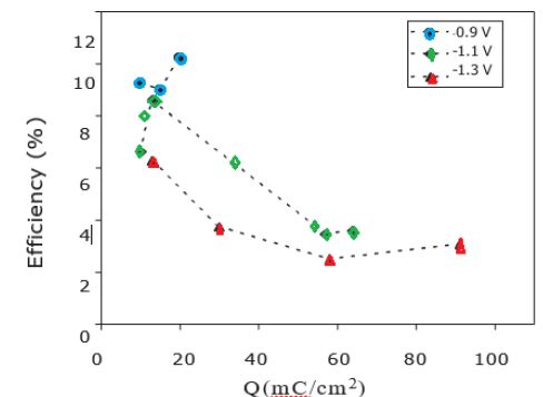
Figure 3: Efficiency of CZS/In2S3-based solar cell as a function of deposition potential and electrical quantity of deposition measured under simulated AM1.5-100 mW/cm2 illumination.
As shown, for very low electrical charge values (<20 mQ/cm2) corresponding to low thickness of In2S3 buffer layers, similar conversion efficiencies are obtained for layers deposited between -1.0 and -1.3 V. However, the conversion efficiency for cells deposited at -1.2V decreases markedly when the electrical charge used for the buffer layer deposition increases. On the contrary, for buffer layers deposited at-0.9 V the efficiency of solar cells increases with the increase of electrical charge. Best results are obtained for a potential of -0.9 V and an electrical charge between 10 and 20 mQ/cm2 with a maximum efficiency of 12.0%.
Figure 4 shows the current voltage curve of one of the best cell prepared at -0.9 V compared to that with CdS (Figure 4b). An improvement of Jsc for cells with In2S3 buffer is observed compared to cells with CdS. For comparison the spectral responses of the cell obtained with In2S3 and that of a cell are shown in Figure 4b. The spectral response displays external quantum efficiencies of about 80% between 450 and 900 nm. Towards short wavelengths, for CdS buffer layers, the quantum efficiency drops from about 500 nm, while for In2S3 buffer layers the drop of the quantum efficiency occurs only at about 380 nm. Such a result confirms the higher value of the apparent bandgap of the In2S3 buffer layers. However for instance the Voc and FF of the solar cells remains lower than the one with CdS buffer layers indicating the non-optimized interface between CIGSe and the ED-In2S3.
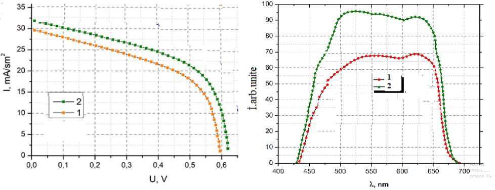
Figure 4: (a) Current-voltage curves for best CZS cells under simulated AM1.5-100 mWcm-2-illumination with a before (1) and after (2) HT (b) Spectral responses measured under short-circuit conditions before (1) and after (2).
Conclusion
Through a systematic study of the deposition parameters of In2S3 layers on Al and CZS solar cells as function of potential of deposition we have achieved a high efficiency of about 12.0%. We observed that, to obtain good efficiencies, the two key parameters are potential of deposition and the thickness of the films. The morphology of films are highly substrate dependent and for higher deposition potential (higher than – 1.1V) and low thicknesses films exhibited good substrate coverage. Solar cells with ED-In2S3 layers present very good photo current densities, but cell performance was limited by the low Voc and fill factor. The low values of the open-circuit voltage and the fill factor of the best cells show that the interface quality between CZS and In2S3 can be more improved.
References
- XH, Xu, et (2011) A novel one-step electrodeposition to prepare single-phase CuInS2 thin films for solar cells. Solar Energy Materials and Solar Cells 95: 791-796.
- Fiechter S (2008) On the homogeneity region, growth modes and optoelectronic properties of chalcopyrite-type CuInS2. Phys Stat Sol (b) 245: 1761-1771.
- Maier E, et (2011) CuInS2–Poly(3-(ethyl-4-butanoate) thiophene) nanocomposite solar cells: Preparation by an in situ formation route, performance and stability issues. Solar Energy Materials and Solar Cells 95: 1354-1361.
- Cui Yanfeng, et al. (2011) Synthesis and characterization of co-electroplated Cu2ZnSnS4 thin films as potential photovoltaic Solar Energy Materials and Solar Cell 95: 2136-2140.
- Sharma R, et (2009) Optimization of growth of ternary CuInS2 thin films by ionic reactions in alkaline chemical bath as n-type photoabsorber layer. Materials Chemistry and Physic 116: 28-33.
- Lee DY, Kim JH (2010) Characterization of sprayed CuInS2 films by XRD and Raman spectroscopy Thin Solid Films 518: 6537-6541.
- Merdes S, et (2011) Influence of precursor stacking on the absorber growth in Cu(In,Ga)S2 based solar cells prepared by a rapid thermal process. Thin Solid Films 519: 7189-7192.