Abstract
Aichi Synchrotron Radiation Center was designed for industrial use in main following discussion among academia, industry and local government in the Aichi area. In addition to the hardware, attention was given to quick and user-friendly use. The unique process for users will be described and the performance for 10 years will be reviewed.
Keywords
Synchrotron radiation, Industrial use, Beamlines, XAFS, Advanced materials
Introduction
The Aichi Synchrotron Radiation Center (AichiSR) started its open use with 6 beamlines on March 26, 2013 and has grown steadily during 10 years to 12 beamlines with over 10,000 hours of used beamtime in the 2022 fiscal year. The facility is owned by Aichi Science & Technology Foundation, which cooperates with industry, academia, and the Aichi Prefectural Government. The AichiSR is responsible for maintenance, operation of the facility, and user services. The AichiSR is the 8th SR facility constructed for public use in Japan as of 2023. Since three general-purpose facilities already exist (Photon Factory, UVSOR, and SPring-8), other facilities can be designed for specific purposes. When we first started discussing on SR facility in the Aichi area in 1991, the Photon Factory and UVSOR were already operating, and construction of the SPring-8 had begun. Therefore, our aim was to construct a compact and easily accessible facility. Based on open seminars carried out in 2000 and 2001, we learned that there were a large number of active SR users in industry and universities in the Aichi area, and some of them expressed a desire to have an SR facility in this area. Considering the needs of industrial and academic researchers, working mainly in the fields of applied physics and chemistry, in 2003 we, Nagoya University SR group, proposed a plan called “Photo-Science Nano-factory”. In this proposal, a center would be constructed with the synchrotron radiation facility as a core facility and providing other high-level measurement and analysis methods such as transmission electron microscopy, scanning electron microscopy, secondary ion mass spectroscopy, nuclear magnetic resonance and so on [1]. The technicians, scientists, and researchers working at the facility would fully support the needs of users. Research laboratories, incubation laboratories, and conference and meeting rooms would also be constructed. This plan attracted the attention of both industry and the Aichi Prefectural Government.
Based on opinions expressed by both industry and academia, the design of the light source was based on a 1.2-GeV storage ring with a booster ring for top-up operation, and 4 superconducting bending magnets (Superbends) for hard X-rays, 8 normal conducting bending magnets (Normal-bends) for soft X-rays, and one undulator for VUV. The working group was made up of members of Nagoya University, members of the Aichi Prefectural Government, and power users from industry and brushed up the design. A plan for implementation of the Nano-factory was completed, and the final report of the “Knowledge Hub Aichi” project based on the Nano-factory was submitted to Aichi Prefecture. In 2009, Aichi Prefecture approved construction, which then started in 2010. In the summer of 2011 the accelerators were installed, and commissioning began in 2012. The first light was observed in the summer of 2012, and the opening ceremony took place on March 22, 2013. The construction costs, 7.2Billion Yen, for the facility were covered by Aichi Prefecture (50%), donations from industry in Japan (20%) and the Japanese National Government (30%). Therefore, from the beginning, the AichiSR facility was a common local and national asset, and is basically open to any researcher without restrictions based on region or country.
Facility Overview
Accelerators
The accelerators consist of a 50MeV LINAC, a 50MeV-1.2GeV booster ring and a 1.2GeV storage ring [2]. The storage energy of 1.2 GeV was chosen based on the desire to construct a compact ring (72m circumference) that could supply hard X-rays (up to about 26 keV) into more than 8 beamlines from 4 Superbends with a magnetic field of 5T [2,3]. The Superbends are cooled by one cryopump for one Superbend without using any liquid He or N2 (there are no coolant vessels), overhauling once a year.
The combination of compactness and the ability to produce both hard and soft X-rays was a basic requirement during the design phase. The booster ring has two purposes. Firstly, it removes the need to ramp up the magnetic field in the bending magnets of the storage ring, thus avoiding any possible nonlinear dependence of the magnetic field in the Superbends on the driving current. Secondly, it allows the storage ring to be run in a top-up mode. Light with the same quality and the same brilliance is required for experimental repeatability and for checking the reproducibility of products that are a strong requirement from industry users. The top-up operation has been conducted from the beginning of the open use. Brilliance curves are shown in Figure 1.
4-hours beamtime is allocated to one shift and two shifts a day are scheduled as (I) 10:00-14:00, and (II) 14:30-18:30, from Tuesday through Friday for users, while the facility is dedicated to machine study on Monday. For most of the experiments 4-hour is long enough since the beamlines and end-stations are set up before users come according to discussion with beamline staff as mentioned in use flow.
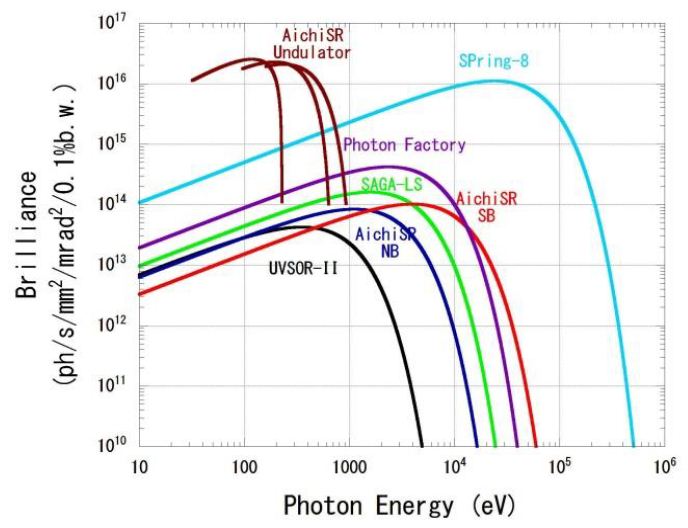
Figure 1: Brilliance curves of the light from Superbend (red), Normal-bend (blue), and undulator (brown) at AichiSR. Those of some other facilities in Japan are also plotted.
Beamlines
In Table 1, the six beamlines constructed at the first stage are: 1) hard X-ray absorption fine structure (XAFS) and fluorescence X-ray analysis (BL5S1: 5~22 keV), 2) tender X-ray XAFS and photoelectron spectroscopy (BL6N1: 1.75~6 keV), 3) ultra-soft X-ray XAFS, vacuum ultraviolet (VUV) and photoelectron spectroscopy (BL7U: 30~1000 keV), 4) powder X-ray diffraction (BL5S2: 5~20 keV), 5) X-ray reflection, thin film and surface diffraction (BL8S1: 9.1, 14.37, 22.7 keV), and 6) wide/small-angle X-ray scattering (BL8S3: 8.2 and 13.5 keV) [4]. These 6 beamlines were selected out of 9 beamlines proposed (other 3 beamlines were protein structure analysis, micro/nano processing, and infrared imaging beamlines) and user demands were investigated using questionnaires from active and potential users and direct hearing from power uses in industry to focus to 6 beamlines.
Table 1: Beamlines open for users at present (Beamlines in italic are the first 6 beamlines)
|
Spectroscopy Beamlines (from 30 eV to 26 keV) |
Diffraction, Scattering, Imaging Beamlines |
| BL7U(VUV, Soft X-ray XAFS, PES)
Energy Range: 30~1000 eV BL1N2(Soft X-ray XAFS, PES) Energy Range: 0.15~2.0 keV BL6N1(Tender X-ray XAFS, PES) Energy Range: 1.75~6.0 keV BL5S1(Hard X-ray XAFS) Energy Range: 5~22 keV BL11S2(Hard X-ray XAFS) Energy Range: 5~26 keV |
BL2S1(Protein (Nagoya University))
Energy: 11.0, 17.2 keV BL5S2(Powder X-ray Diffraction) Energy Range: 5~20 keV BL8S1(Thin Film Diffraction) Energy: 9.1, 14.37, 22.7 keV BL8S3(Wide/Small Angle X-ray Scattering) Energy: 8.2, 13.5 keV, Camera Length: 0.2~6.4 m BL8S2(X-ray Topography, X-ray CT) Energy Range: 7~24 keV |
Fortunately, protein structure analysis beamline (BL2S1) was constructed by Nagoya University using a supplementary budget from the Japanese Government, nano processing and imaging beamline (BL8S2) by an Aichi Prefecture Research Project.
Demand for the hard X-ray XAFS beamline was high and 2 beamlines maybe necessary from the beginning. It turned out to be true and BL5S1 reached to 100% of available beamtime. Then, BL11S2 was constructed by Aichi Prefecture Government.
BL2S1 and BL11S3 in Table 2 were constructed by a private company in Aichi. The number of beamlines became twice of the first 6 beamline within 10 years.
Table 2: Beamlines owned by a private company
| BL2S3 (Hard X-ray XAFS and X-ray diffraction)
BL11S3 (X-ray CT) |
In Figure 2, yearly change of the beamtime, with fraction of user category (Big, Medium/small-companies, Industry-Academia collaboration, Universities, and Public Research Institutes), beamlines, and beamtime used for measurement acting service (red line). Influence of COVID-19 is clear in 2020 and 2021, that is the saturation of used beamtime (not dipped) and steep increase of the beamtime used for measurement active service. We carefully controlled the infection path (without shut-down of facility) and there was no infection at AichiSR.
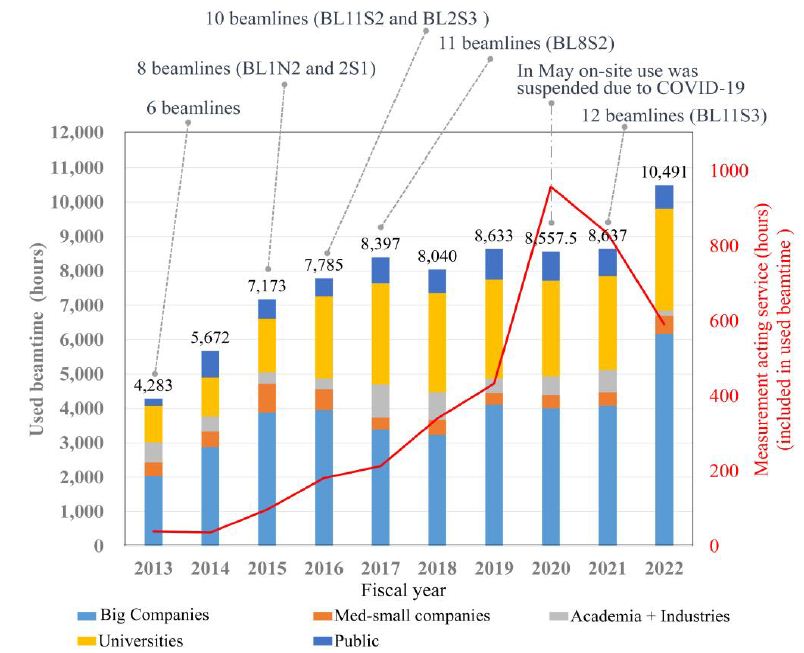
Figure 2: Yearly change of beamlines and beamtime used
Measurement Acting Service
Measurement acting service is common for most of the facilities. In AichiSR, especially for soft X-ray or VUV absorption experiments, a transfer vessel was developed before COVID-19 to keep samples under a high vacuum or in a high purity inert gas while transferring them to high-vacuum/high-purity chambers at AichiSR. User can send the vessel to or carry in AichiSR. The vessel was designed to be used by other member facilities of the project “Photon-Beam Platform” for different experiments at different beamlines in Japan [5].
Beamtime Assignment Process
The key factors that were considered with regard to industrial use are: 1) ease of use (low threshold for entry), 2) measurements under in-situ and in-operand conditions, 3) repeated experiments on the same topic, 4) short time from application to execution, and 5) nondisclosure of results. To realize 4), applications are accepted every two months. All users pay for beamtime, but the charge is much lower for academic use under the condition that results are disclosed. It turned out those factors (from 1~4) are quite convenient for academic users too.
To realize those key factors the use-flow as shown in Figure 3 is taken at our facility. (1) Consultation: contact to our consultation office to discuss details of your experimental plan and with coordinator and if necessary with beamline staff. (2) applications are accepted every two months. (3) Decisions on usage follow a first-come-first-served basis. The review process for proposals focuses on safety and technical possibility rather than evaluation. Allocation of beamtime is informed within two weeks. When there is a vacancy of the beamtime, it is announced and allocation is made within one week at the shortest. (4) Necessary to complete several forms for use, such as radiation worker registration application form, radiation worker approval certificate, written pledge, and so on. (5) At the reception desk you can obtain an entry card and a personal radiation measurement badge. (6) Prepared samples are mounted on the sample stage. Beamline instruments are usually adjusted and checked by our beamline staff members (two per one beamline and all of them are PhD holders) before your beamtime. Support on instrument operation, sample measurements, and necessary assistance are provided. Analysis support can also be provided within the beamtime, and (7) after the experiments, signing a form of completion, return of entry card, and radiation badge to the box at the reception desk are required.
For university and public institute users, experimental results have to be reported in a form within 50 days after the experiment. This disclosure of the results allows a much lower fee (half) than that of big company (fee for medium-small sized company is also a half to encourage their usage). If academic users pay the full fee, disclosure of results is exempted.
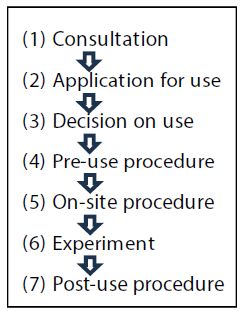
Figure 3: Use flow
Industrial Use
In 2022, 65% of our users were from industry (including industry-academia collaborations), 28% was purely academic and the remainder was from public research institutes, as shown in Figure 4. The research fields of these users were very diverse, as shown in Figure 5. The fraction is almost unchanged during 10 years. The beamtime increased by about twice as can be seen in Figure 1.
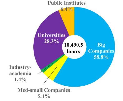
Figure 4: AichiSR users from industry, universities and public research laboratories in 2022 of 12 beamlines. The fraction is almost unchanged during 10 years. The beamtime increased by about twice as can be seen in Figure 1.
As can be seen in Figure 5, production type of industry is diverse, but 50% of users are related to R&D for automobiles. Chemicals, Research services, or Electronic devices come next. Though the fraction is smaller, users from quite a wide variety of research fields come to use AichiSR.
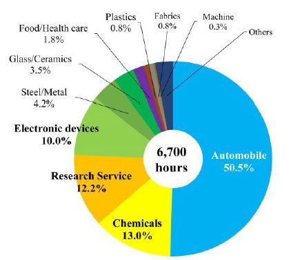
Figure 5: Fraction of production type of industry. Beamtime used by automobile and related R&D is 50% and has been top for last 10 years. Chemicals, Research service, or Electronic devices comes next changing year by year. The beamtime is of industrial use only.
The goal of industrial research is not to publish papers, but to produce profitable products. Therefore, evaluation of proposals for beamtime should not be performed based on scientific importance or impact on novel technology. Repeated experiments are also important in industry.
Beamline and beamtime assignments are carried out through negotiation between coordinators and users as described above. Use of multiple beamlines for one application is possible, and sometimes we actually suggest this to users.
Use Situation of Beamlines
Popularity of Beamlines
Figure 6 shows the fraction of usage techniques by 10 open-use beamlines at AichiSR in 2022. There are 5 beamlines that cover the energy from 30eV to 26keV without gaps as listed in Table 1. Hard X-ray XAFS (BL5S1 and BL11S2) covers 26%, soft X-ray XAFS (BL1N2 and BL6N1) covers 23% of the beamtime, thus XAFS measurement occupy 49%. 58% of the beamtime is used for absorption measurements when the VUV (BL7U) is included. It is well recognized that AichiSR is strong for the XAFS measurements. XAFS has been used to develop new materials to obtain new functions and new devices, such as exhaust catalysts, Li-ion batteries, semiconductors, nanoparticles, and many others.
Current problem is that most of the beamlines are full almost all through the year. Especially in the last quarter of each year the applied beamtime overflows from the available time of XAFS beamlines. Construction of new beamlines and modification of other less busy beamlines are being seriously discussed.
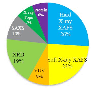
Figure 6: Usage faction of measurement techniques in 2022
An Example of XAFS Measurement
An example of XAFS measurement is shown in Figure 7. The native passive film structure on SUS304 surface was investigated using Hard-X-ray XAFS, (BL5S1) and photoelectron spectroscopy (XPS, BL6N1 and BL7U). The XAFS spectra clearly showed an ordered network-structure (at least<1nm) of Cr(IV) oxide. In addition, the XPS spectra indicated that the chromium oxide was transformed into a chromium oxyhydroxide such as a -O-Cr-OH- structure. Fourier-Transformed EXAFS spectra of the SUS304 substrate and the two reference samples are shown in Figure 7. The measured energy range of 5690-7084eV that is the k range of 0-16.9 Å-1. The overlapped curve to the measured spectrum shows the simulated spectrum using the FEFF method.
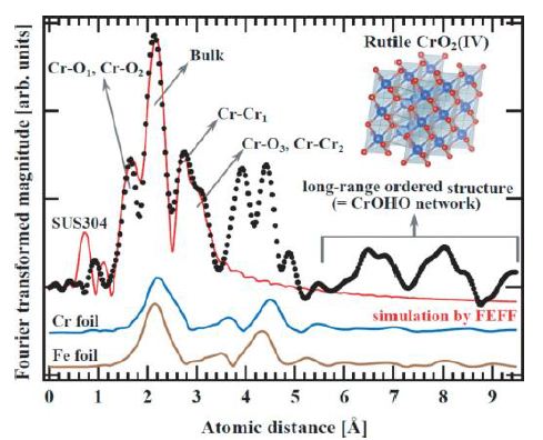
Figure 7: FT-EXAFS spectra of the SUS304
Figure 8 shows a new structural model of the native passive film on the SUS304 substrate obtained by the experiments described above. The left and right figures show a Cr-terminated structure and an OH/O terminated one, respectively [6].
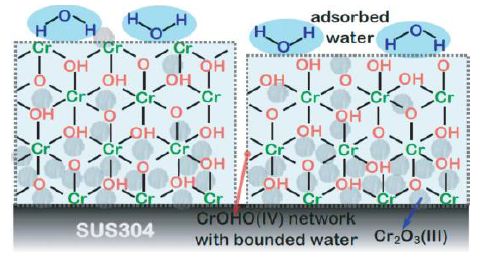
Figure 8: Structure model of the native passive film
Summary
After 10 years of discussion and planning by universities, industry, and local government in the Aichi area, the Aichi Synchrotron Radiation Center was designed for industrial and academic use. The choice of accelerators, beamlines, and service management was determined based on discussion and feedback involving industry and academia. Of the six beamlines available, the highest priority was given to XAFS beamlines that allow analysis of elements from Li to U. In addition to the hardware, attention was given to the development of operating procedures that were quick and user-friendly. The facility became available for public use in March 2013. In 2013, 55% of the experiments involved XAFS analysis (hard X-ray, soft X-ray and VUV regions). 6 beamlines increased to 12 beamlines and the used beamtime also increased twice of the first year. The beamtime allocated to industrial use increased from 2,976 hours in 2013 to 6,700 hours in 2022. The range of research fields for users of the facility was found to be very broad, and the beamtime used by automobile and related R&D is 50% and has always been top at AichiSR.
References
- Takashima Y, Yamane T, Takeda Y, Soda K, Yagi S, et al. (2007) AIP Conference Proceedings (American Institute of Physics) 879: 75-78.
- Yamamoto N, Takashima Y, Hosaka M, Morimoto H, Takami K, et al. (2010) Proceedings of IPAC2010 (Kyoto Japan) 2567-2569.
- Yamamoto N, Takashima Y, Hosaka M, Takami K, Mano A, et al. (2011) Proceedings of IPAC2011 (San Sebastian, Spain) 2987-2989.
- Yamamoto N, Takashima Y, Katoh M, Hosaka M, Takami K, et al. (2010) The 10th International Conference on Synchrotron Radiation Instrumentation (Melbourne, Australia, American Institute of Physics) 591-594.
- Nakanishi Y,Yagi S, Ohta T (2010) IEEJ Electronics, Information and Systems 130: 1762-1767 (in Japanese).
- Shimizu S, Ito S,Asaoi H, Miyamawa T, Muto M et al. (2016) Hyomen Kagaku 37: 422-428 (in Japanese).